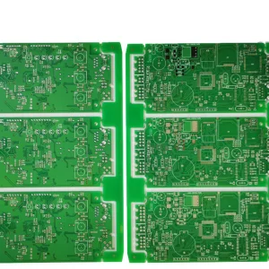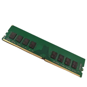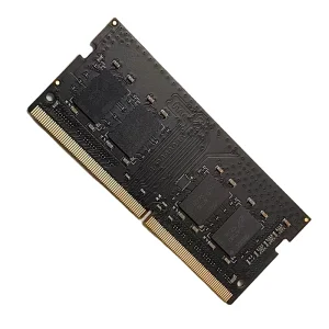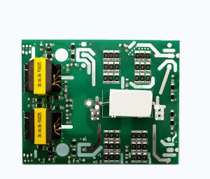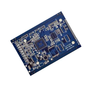
The global semiconductor and electronics hardware manufacturing industries are undergoing a massive transformation. The rapid emergence of Artificial Intelligence (AI) datacenters, high-performance computing (HPC) nodes, automotive electronics (especially EV powertrain control), and smart industrial automation systems has placed unprecedented demands on Printed Circuit Board (PCB) manufacturers and suppliers. High-Speed, High-Layer Count (HLC) boards, High-Density Interconnect (HDI) designs, and specialized substrates are no longer niche products; they have become the bedrock of the modern digital economy.
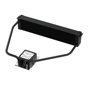
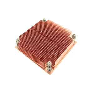
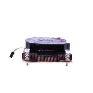
Currently, global engineering teams face stringent challenges regarding signal attenuation, heat dissipation, and board integrity. For instance, the migration from DDR4 memory architectures to DDR5 architectures requires PCBs with incredibly low signal loss, precise trace-width controls, and minimal electromagnetic interference (EMI). Additionally, as CPUs and GPUs scale beyond 300W to 400W TDP, thermal engineering must be built directly into the electronics hardware through integrated copper bottom heatsinks, vapor chambers, and advanced liquid cooling blocks.
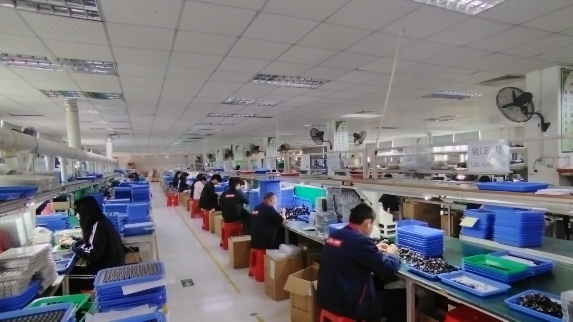
When global organizations seek a PCB supplier, China remains the epicenter of efficiency, capacity, and advanced technological execution. This structural dominance is not merely based on labor costs; rather, it is driven by deep ecosystem integration, robust logistical infrastructures, and rapid prototyping capabilities. The South China electronics manufacturing clusters (spanning Shenzhen, Dongguan, and Guangzhou) allow factories to source copper-clad laminates (CCL), specialized solder paste, high-speed SMT placement nozzles, and testing instrumentation within a 50-kilometer radius.
What takes weeks in Western markets is executed within 24 to 48 hours in Shenzhen SMT facilities. Rapid design validation reduces time-to-market exponentially.
From Immersion Silver (ImAg) to Electroless Nickel Immersion Gold (ENIG), Chinese surface finishes ensure exceptional shelf life and superb joint reliability for fine-pitch BGAs.
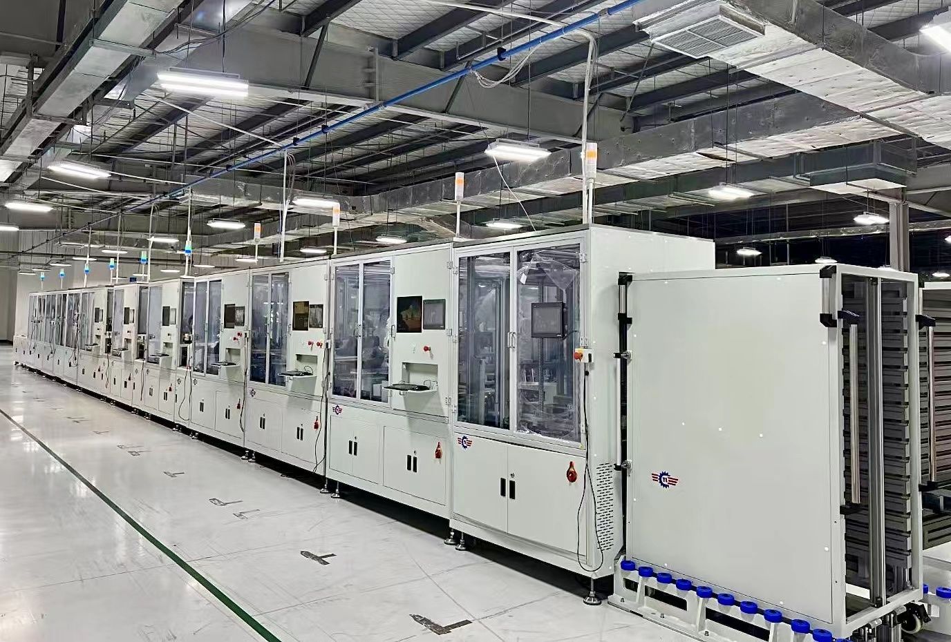
High-volume automatic production lines lower the cost per unit, ensuring global system integrators maintain strong gross margins without sacrificing quality.
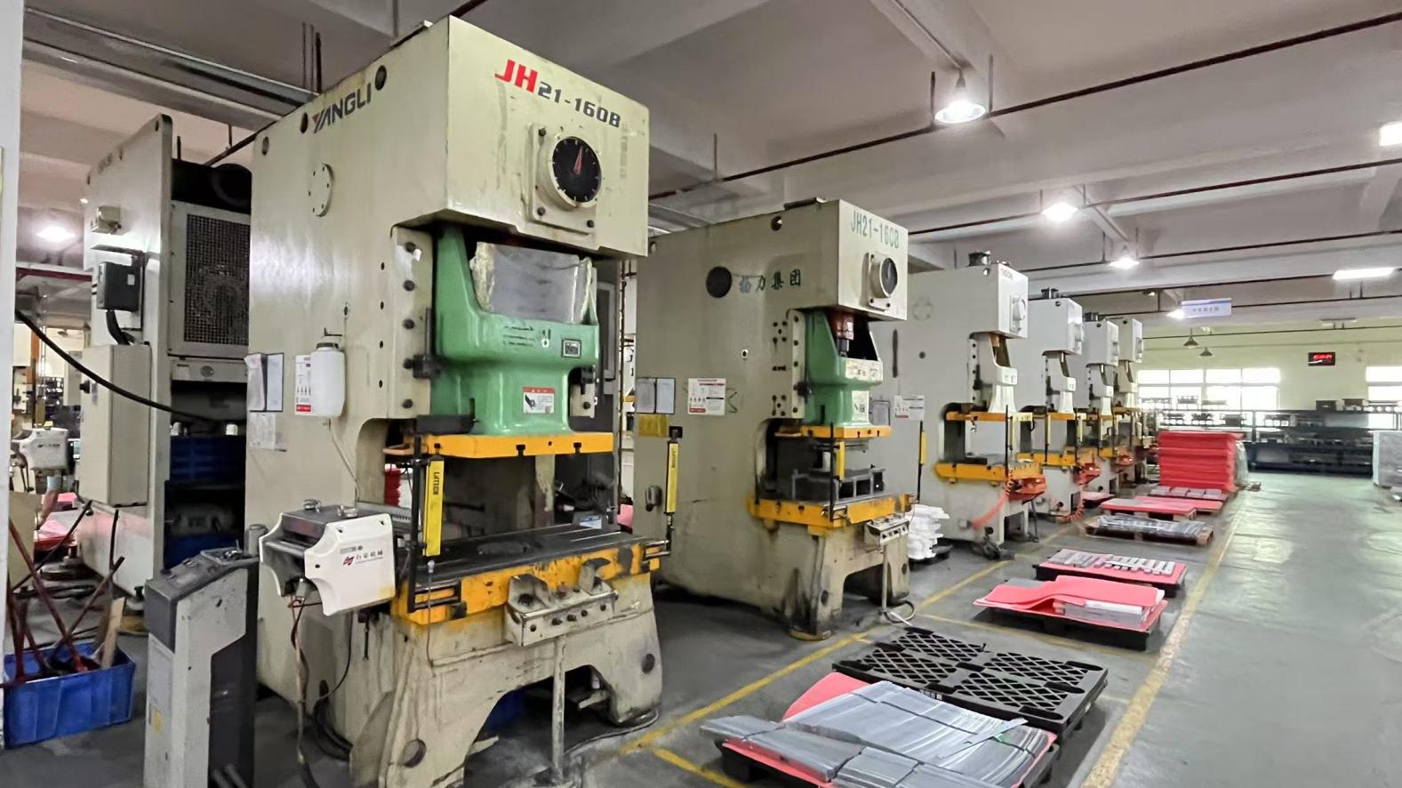
By leveraging state-of-the-art automatic visual inspection (AOI), in-circuit testing (ICT), and functional testing (FCT), Chinese factories bridge the gap between design theory and mass production reality. This creates a highly reliable supply chain suitable for aerospace, defense, telemetry, consumer computing, and industrial machinery.
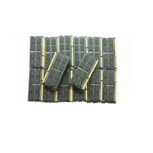
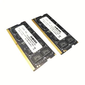
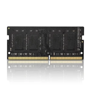
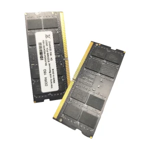
Founded in 2016, Kryntel Memory Technology (China) Co., Ltd. is a professional DDR5 memory manufacturer specializing in high-performance RAM modules for global OEM, ODM, and private label partners. With a modern production facility covering approximately 320㎡, we focus on delivering stable, high-speed, and energy-efficient memory solutions for gaming, industrial, and server applications.
Over the years, Kryntel has built strong export capabilities with annual export revenue ranging from USD 8 million to USD 18 million. The company has accumulated 6 years of export experience and 9 years of overall industry experience in memory and semiconductor-related manufacturing. Our main customer base includes computer hardware brands, system integrators, distributors, and e-commerce sellers globally.
We cooperate with a global supply chain network of approximately 1,200 upstream and downstream partners, ensuring stable sourcing of high-quality DRAM chips and components. This extensive supply chain footprint, paired with our engineering capabilities, guarantees that Kryntel can mitigate supply disruptions and offer competitive pricing.
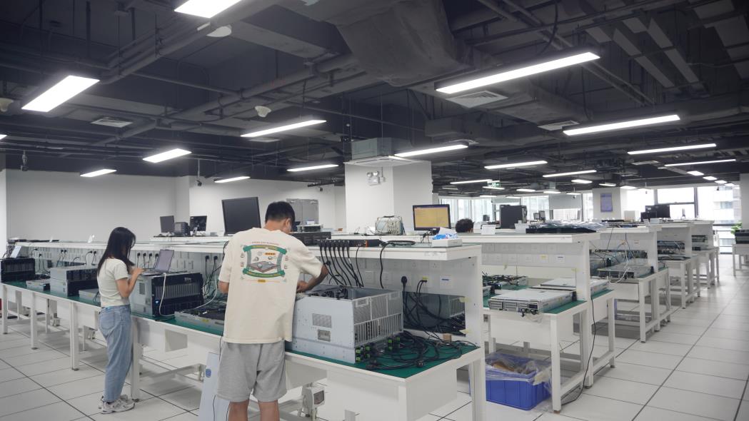
Our quality control system is built on strict multi-stage inspection standards, including incoming material inspection, in-process quality control, aging tests, and final product sampling inspection. Product testing methods include high-temperature aging tests, compatibility testing with major motherboard platforms, bandwidth stress testing, and voltage stability testing. We maintain a dedicated QA team of 42 professionals to ensure consistent product reliability.
| Testing Stage | Methodologies Employed | Objective |
|---|---|---|
| Incoming Quality Control (IQC) | X-ray Fluorescence (XRF), Solderability testing, Visual microscopy | Verify alloy purity, ensure lead-free compliance, and inspect incoming DRAM dies. |
| In-Process Quality Control (IPQC) | 3D Solder Paste Inspection (SPI), Automated Optical Inspection (AOI) | Detect pad misalignment, dry joints, and bridge formations in real time. |
| Post-Assembly Stress Testing | High-temperature burn-in chambers (60°C to 85°C), Voltage sweep testing | Accelerate infant mortality failures to guarantee stable long-term field operation. |
| Platform Compatibility Validation | Multi-vendor BIOS validation, memtest86+ cycles, OS environment boots | Ensure cross-platform stability across Intel, AMD, and major server chipset ecosystems. |
Our R&D department is highly capable, supporting advanced customization, including PCB design optimization, frequency tuning, heat dissipation solutions, and branding customization. We offer full OEM/ODM services with flexible customization options such as frequency, latency, heat spreader design, packaging, and firmware tuning.
In the past year, we successfully launched over 280 new memory products across DDR4 and DDR5 series. Our R&D team consists of approximately 160 engineers specializing in memory architecture, signal integrity, and product reliability optimization.


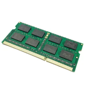
The hardware landscape is shifting rapidly. The emergence of DDR5 RAM has fundamentally altered PCB layout paradigms. Unlike DDR4, where the Power Management Integrated Circuit (PMIC) resided on the motherboard, DDR5 places the PMIC directly on the memory module's PCB. This design change reduces voltage drops and trace complexities on the motherboard but increases heat generation and routing density on the memory module itself.
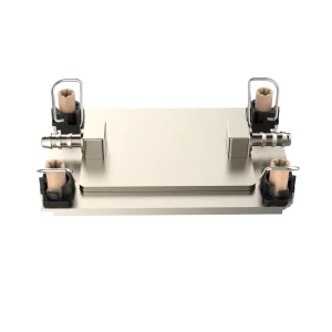
Consequently, modern PCB suppliers must deploy sub-mil trace precision, low-dielectric constant (Dk) materials, and low dissipation factor (Df) copper foils. If signal integrity is compromised, the high data transfer rates of 4800MHz to 6400MHz and beyond will suffer from high bit error rates. Concurrently, thermal structures are shifting from standard passive aluminum fins to complex hybrid systems. The application of high-wattage processor configurations has rendered liquid cooling modules (such as LGA4677 block systems) essential in keeping server operating temperatures below throttle thresholds.
For enterprise purchasing agents, hardware manufacturers, and system integrators located in North America, Europe, and Asia, sourcing printed circuit board assemblies and memory units requires careful consideration. A mistake in trace sizing or a batch of sub-par DRAM dies can halt entire manufacturing lines. Key sourcing strategies include:
 Kryntel