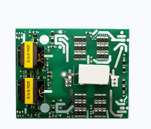
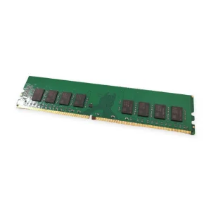
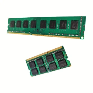
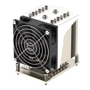
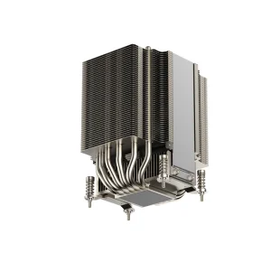
Explore our curated selection of high-frequency printed circuit boards, high-speed DRAM memory structures, and advanced CPU server interfaces engineered for optimal signal processing and low dielectric losses.
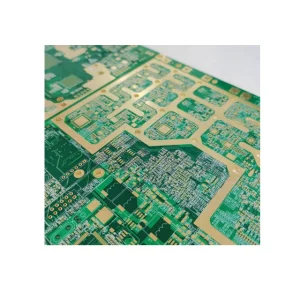
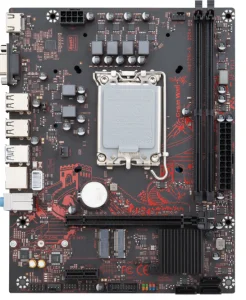
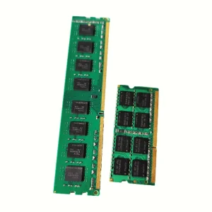
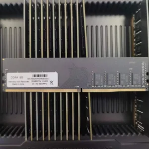
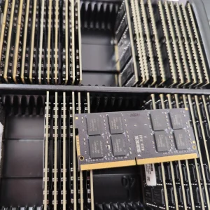
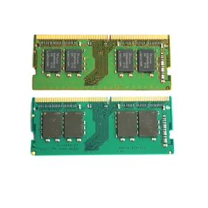
In high-frequency signal transmission, the printed circuit board (PCB) ceases to be a simple structural carrier and acts instead as a critical, distributed-parameter passive component. As operating frequencies scale into the gigahertz (GHz) spectrum—essential for modern 5G/6G infrastructures, satellite communications, and high-performance server architectures—signal degradation mechanisms such as skin effect losses, impedance mismatches, and dielectric attenuation become dominant.
Understanding the physics of signal propagation requires analyzing key material constants: the Dielectric Constant (Dk, εr) and the Dissipation Factor (Df, tan δ). While standard FR4 materials are suitable for low-frequency operations, their relatively high and unstable Dk (>4.2) and Df (~0.02) yield massive signal dispersion and thermal dissipation at higher frequencies. This necessitated the development of specialized high-frequency substrates.
Advanced designs utilize substrates such as PTFE (Polytetrafluoroethylene), ceramic-filled hydrocarbons, or specialized thermoset resins. Industry standards like Rogers 4000 series (e.g., RO4003C, RO4350B) offer exceptionally low Df (down to 0.0037) and highly stable Dk values across dynamic thermal and frequency ranges.
To achieve economic viability without sacrificing electromagnetic integrity, systems integrators deploy hybrid stacks. By pressing high-frequency layers (such as Rogers) on top of cost-effective base layers (like Shengyi FR4 High TG170), engineers optimize outer layer routing for RF lines while burying low-frequency control channels in traditional substrates.
Signal integrity relies heavily on maintaining a strict impedance tolerance (typically ±5% or ±10%). Additionally, copper roughness at the substrate interface dictates the skin-effect loss. Advanced fabricators utilize reverse-treated copper foils (RTF) alongside flat finishes like ENEPIG to preserve trace geometry.
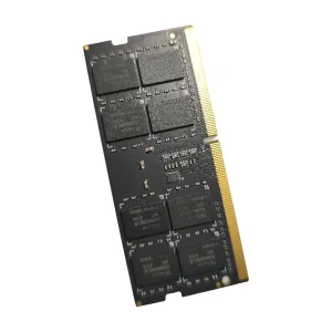
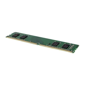
Founded in 2016, Kryntel Memory Technology (China) Co., Ltd. stands as a premier designer and manufacturer of high-performance DDR5/DDR4 memory architectures and advanced semiconductor integration hardware. Crucially, the physical layer constraints that dictate high-frequency PCB manufacturing directly govern the operational stability of high-speed memory systems. High-frequency signal integrity, cross-talk mitigation, and thermal stability are the core areas where memory module architecture meets PCB fabrication.
Spanning a highly optimized production facility, Kryntel implements multi-tiered testing protocols including high-temperature aging tests, platform compatibility testing, stress-testing under extreme bandwidth loads, and voltage swing tests. Our QA team of 42 certified professionals manages every validation point.
With 9 years of deep industry expertise, Kryntel supports extensive hardware customization: PCB dielectric profiling, signal trace design optimization, thermal management layouts, latency matching, and tailored cooling solution interfaces. In the last year alone, we launched over 280 advanced memory designs.
Operating with a comprehensive supply chain, Kryntel services top-tier system integrators, server builders, and industrial automation clients across North America, Europe (especially Germany), India, Brazil, and the Middle East (UAE). We secure direct-from-source DRAM allocations for consistent quality.
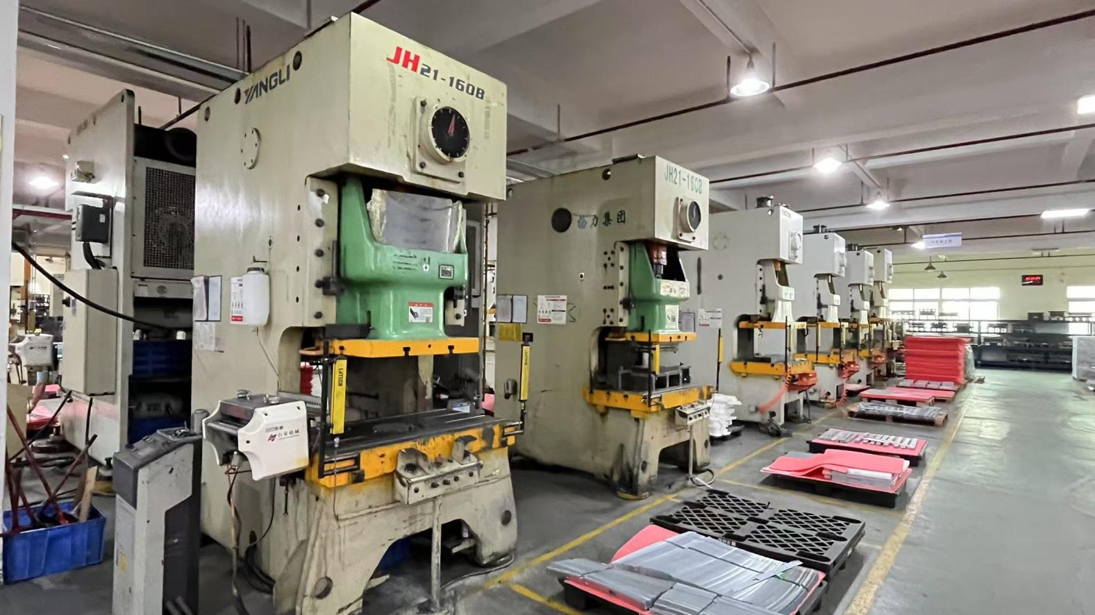
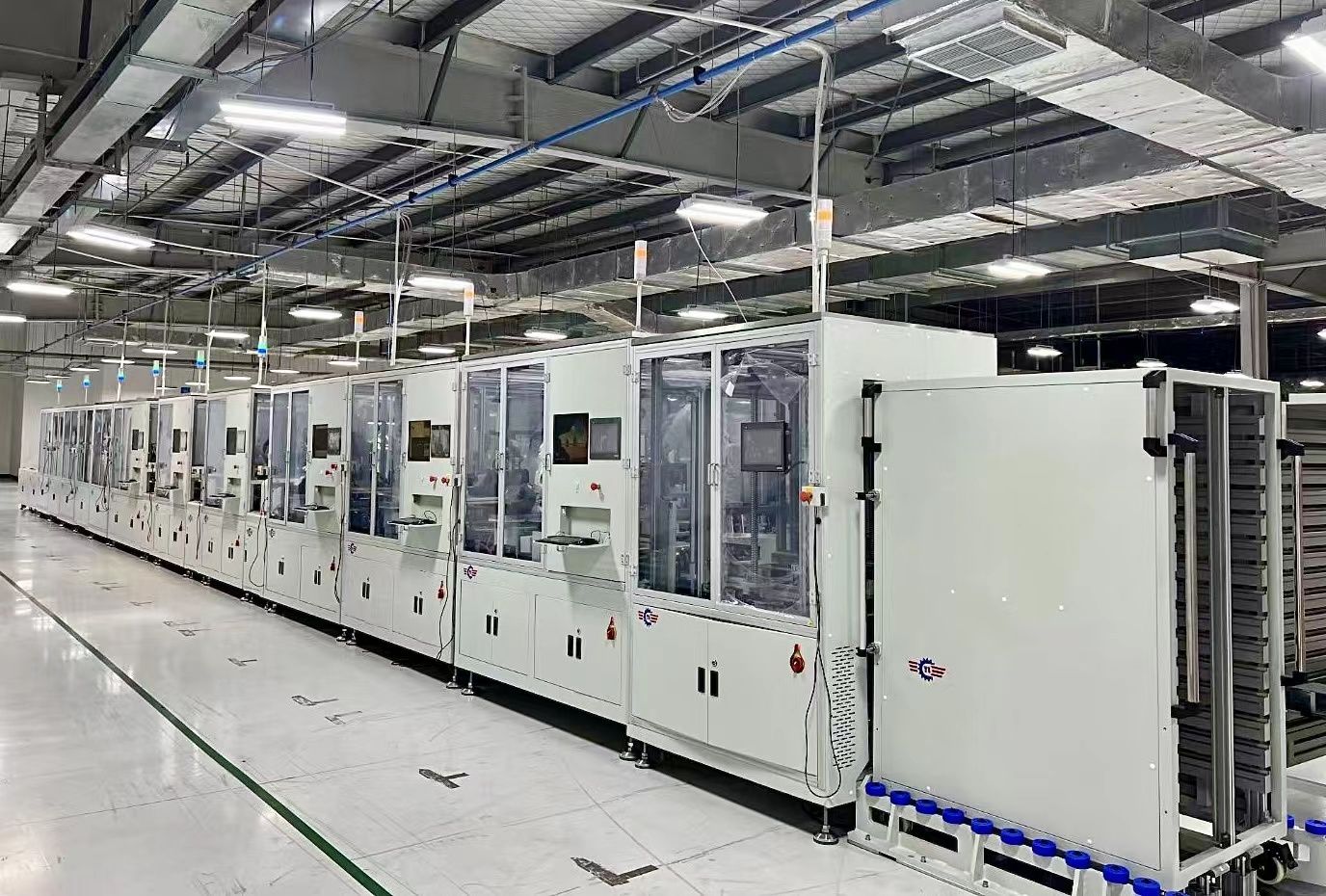
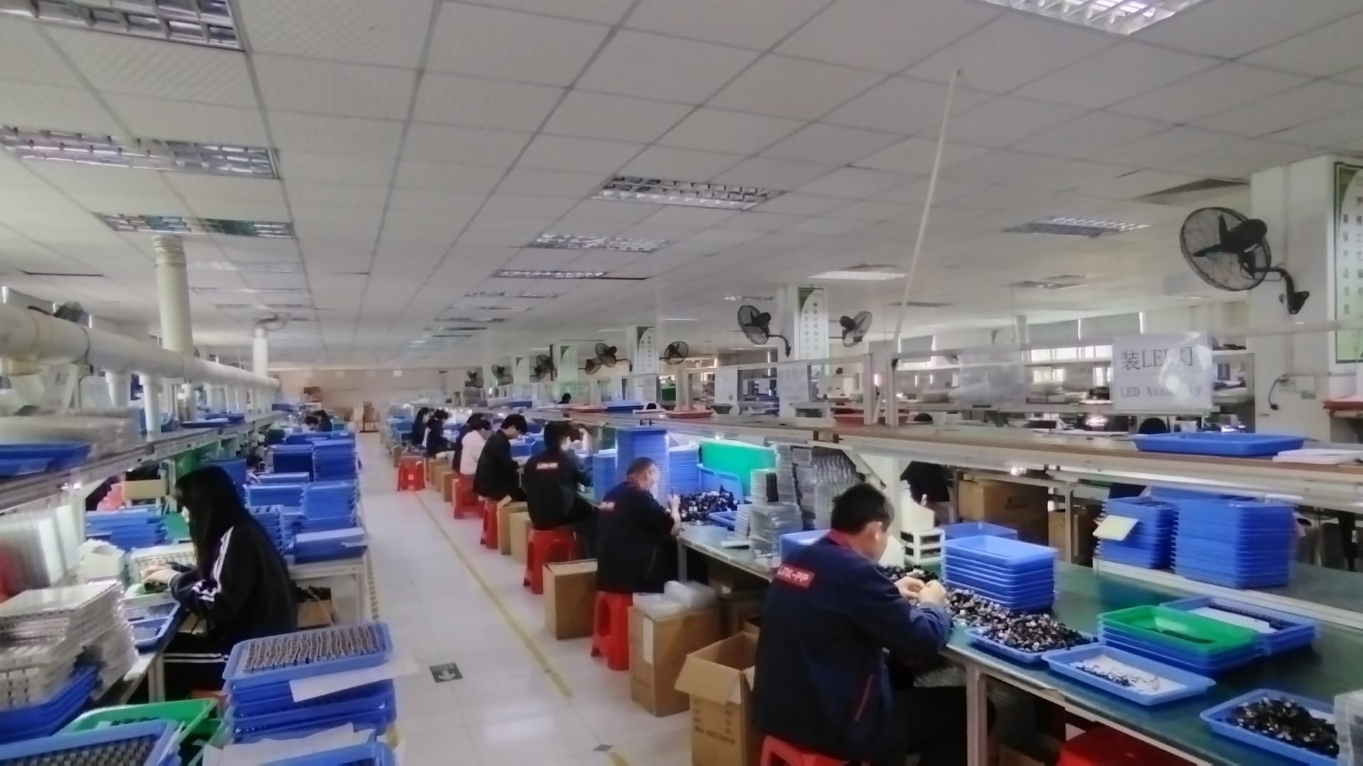


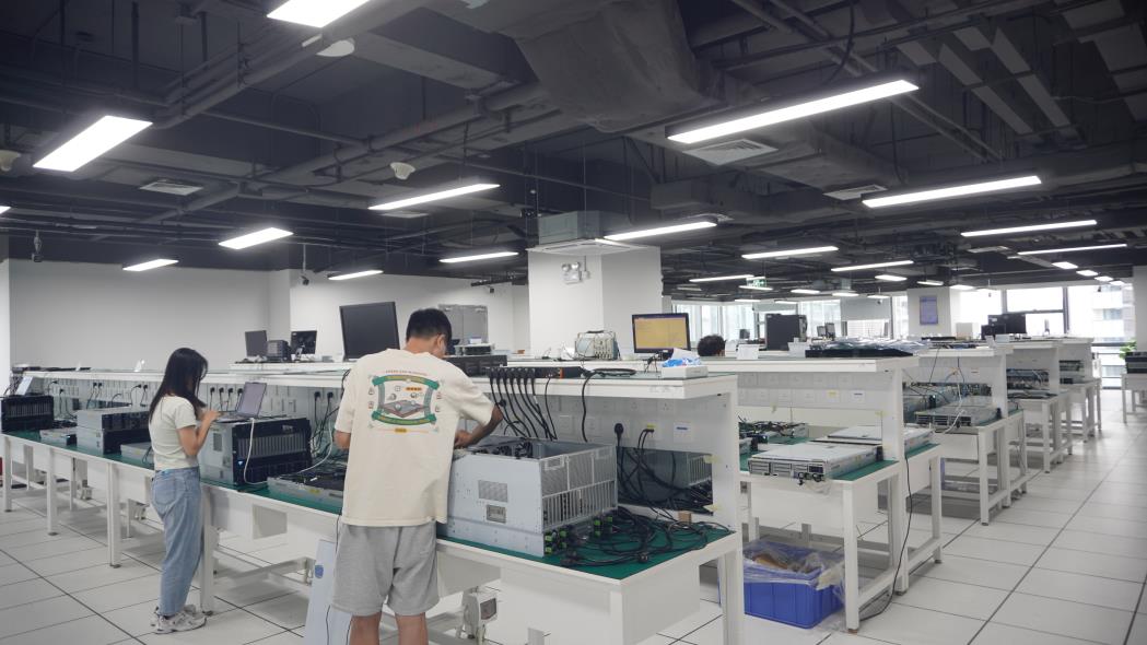
China has established itself as the global epicenter for printed circuit board fabrication, combining unparalleled raw material availability with highly advanced lithography, layering, and testing facilities. For international procurement managers, sourcing high-frequency PCBs from China yields major strategic advantages across the product lifecycle:
Chinese industrial clusters (e.g., Guangdong, Jiangsu) host immediate access to critical chemical agents, fiberglass substrates, electro-deposited copper foils, and premier laminate suppliers. This proximity minimizes raw material lead times and insulates overseas buyers from supply chain shocks.
Equipped with state-of-the-art laser direct imaging (LDI), automatic mechanical drilling, and multi-layer optical target registration systems, Chinese facilities easily construct dense layouts featuring microvias, stacked blind/buried vias, and precise cavity board profiling.
By deploying automated impedance testing, flying probe testers, time-domain reflectometry (TDR), and 3D X-ray systems, manufacturers verify dielectric consistency and trace accuracy. This ensures IPC-Class 3 standard compliance for mission-critical operations.
High-frequency and high-speed PCBs act as the backbone for complex, data-heavy systems. Let's look at the key industrial applications demanding strict impedance controls and ultra-low dielectric loss matrices.
Massive MIMO antennas, 5G base stations, satellite transceivers, and microwave link backhauls running on Rogers or Taconic substrates for minimum signal loss.
77GHz radar arrays, Advanced Driver Assistance Systems (ADAS), and vehicle-to-everything (V2X) wireless nodes requiring extreme reliability and zero-defect thermal behavior.
AI servers, cloud computing motherboards (LGA1700, LGA4677), and next-gen DDR5 arrays where signal pathways are engineered to resist high frequency cross-talk.
High-efficiency power switching converters, welding machine control drivers, and high-frequency inverters requiring precise, high-thermal threshold layouts.
When evaluating suppliers for high-frequency circuit boards, procurement teams must look past basic unit costs to ensure comprehensive manufacturing competency. Use this technical checklist to assess capabilities:
Ensure the supplier maintains formal supply contracts with recognized raw laminate makers (Rogers, Taconic, Shengyi, Nelco). Material traceability documentation must accompany every production batch to prevent counterfeit or degraded stock.
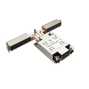
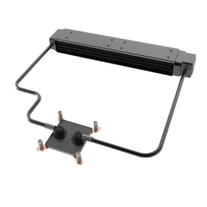
High-frequency modules generate localized thermal hot spots. Verify if the factory offers metal-core PCBs (MCPCB), thick-copper power layers, and direct-integration paths for cooling interfaces, such as aluminum heat sinks and CPU cooling systems.
Confirm that the vendor performs 100% coupon-level impedance validation. Every shipment should include a TDR testing report showing that the impedance curves for differential pair traces fall within the specified ±5% tolerance margins.
The rapid evolution of high-speed systems pushes high-frequency design boundaries forward. As frequencies transition toward sub-terahertz regimes for advanced radar and early 6G trials, three core trends are reshaping substrate production:
Development is shifting toward LCP (Liquid Crystal Polymer) and modified polyimides (MPI). These thin films present exceptional dielectric consistency and low moisture absorption, making them ideal for high-density flex designs in smartphones and aerospace equipment.
To combat signal losses along longer copper traces, engineers are embedding passive components (capacitors, inductors) and active silicon chips directly within inner PCB layers. This shortens signal loops, stabilizing high-speed data streams.
In ultra-scale data centers, electrical routing on PCBs is hitting optical performance limits. Emerging high-frequency architectures integrate fiber-optic routing paths on the PCB substrate itself, transferring data optically directly to the silicon package.
Review technical explanations from our engineering team regarding high-frequency materials, fabrication capabilities, and reliability standards.
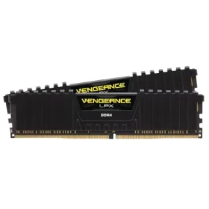
Discover our industrial server components, high-density DRAM modules, and advanced heat dissipation systems designed to maintain platform stability under heavy high-frequency computing loads.
 Kryntel