Explore our core collection of precision engineered boards, processing radiators, and advanced memory modules.

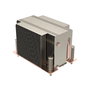

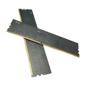
Analyzing current global demand, market vectors, and infrastructure shifts requiring advanced stack-up boards.
The global electronics sector is undergoing a massive shift towards high-frequency, high-density computing architectures. Multi-layer Printed Circuit Boards (PCBs) act as the structural framework for these developments. As IoT devices, 5G networking nodes, electric vehicles (EVs), and AI server clusters expand globally, standard double-sided boards no longer meet the electrical requirements. Multi-layer configurations (ranging from 4 to 32+ layers) are now essential for modern high-speed circuit designs.
By routing signals through inner conductive layers, design engineers achieve high shielding, controlled impedance, and significantly lower EMI (electromagnetic interference). These qualities are necessary for mission-critical industrial hardware, such as WIFI-controlled power bank assemblies, high-current power inverters, and heavy-duty welding machine systems.
Globally, procurement teams face complex supply chain dynamics. Lead times, raw material quality (especially specialized FR-4 TG170/TG180, Rogers, and polyimide materials), and reliable international logistics determine a project's speed-to-market. Kryntel Memory Technology addresses these needs by integrating expert engineering designs, strict quality assurance frameworks, and robust global exporting structures to support complex electronics deployments.
Deep engineering insights into thermal management, substrate choices, and impedance control.
As board layer counts increase, thermal expansion and signal attenuation become critical design challenges. Signals operating in the gigahertz range suffer from dielectric loss and skin effect resistance, requiring careful selection of substrates, copper weights, and layout geometry.
Utilizing microvias, blind vias, and buried vias allows our engineering teams to optimize layout density. This approach reduces overall board size while preserving routing channels for complex high-pin-count BGA chips (such as those in server RAM and processor modules).
Precise impedance calculation (typically 50Ω single-ended and 90Ω/100Ω differential pairs) ensures reliable signal transmission without reflections. This is critical for high-speed protocols like PCIe Gen 5, DDR4, and DDR5 interfaces.
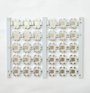
By using heavy copper cores (2oz to 6oz) and aluminum-backed substrates for power components, we ensure that heat is dissipated efficiently away from active components, protecting hardware from thermal degradation.
| Material Type | Dielectric Constant (Dk) @ 1GHz | Dissipation Factor (Df) @ 1GHz | Glass Transition Temp (Tg) | Primary Application Fields |
|---|---|---|---|---|
| Standard FR-4 | 4.2 - 4.7 | 0.015 - 0.020 | 130°C - 140°C | Consumer Electronics, Mid-range Multi-layer Boards |
| High-Tg FR-4 (TG170+) | 4.0 - 4.3 | 0.010 - 0.015 | 170°C - 180°C | Industrial Automation, Server Boards, High-power Inverters |
| Halogen-Free Low Dk/Df | 3.6 - 3.9 | 0.004 - 0.007 | 170°C | DDR5 Memory Modules, Telecom Nodes, High-speed Computing |
| Ceramic/PTFE (Rogers) | 2.2 - 3.0 | 0.001 - 0.003 | 280°C | RF, Microwave, Aerospace, Satellite Communications |
Why manufacturing in China's industrial core ensures lead-time stability and cost-efficiency.
China's PCB manufacturing ecosystem provides access to raw materials, specialized chemical supplies, and high-precision testing machinery. This infrastructure enables rapid iteration from prototype to full-scale production. Kryntel integrates into this ecosystem, maintaining strong partnerships with approximately 1,200 upstream and downstream suppliers to secure high-quality laminates, solder masks, and chemical plating components.
This localized supply chain structure protects operations from global material shortages. By sourcing directly from nearby raw component producers, we minimize logistics transit times, helping customers lower lead times and reduce freight costs compared to suppliers without localized logistics networks.
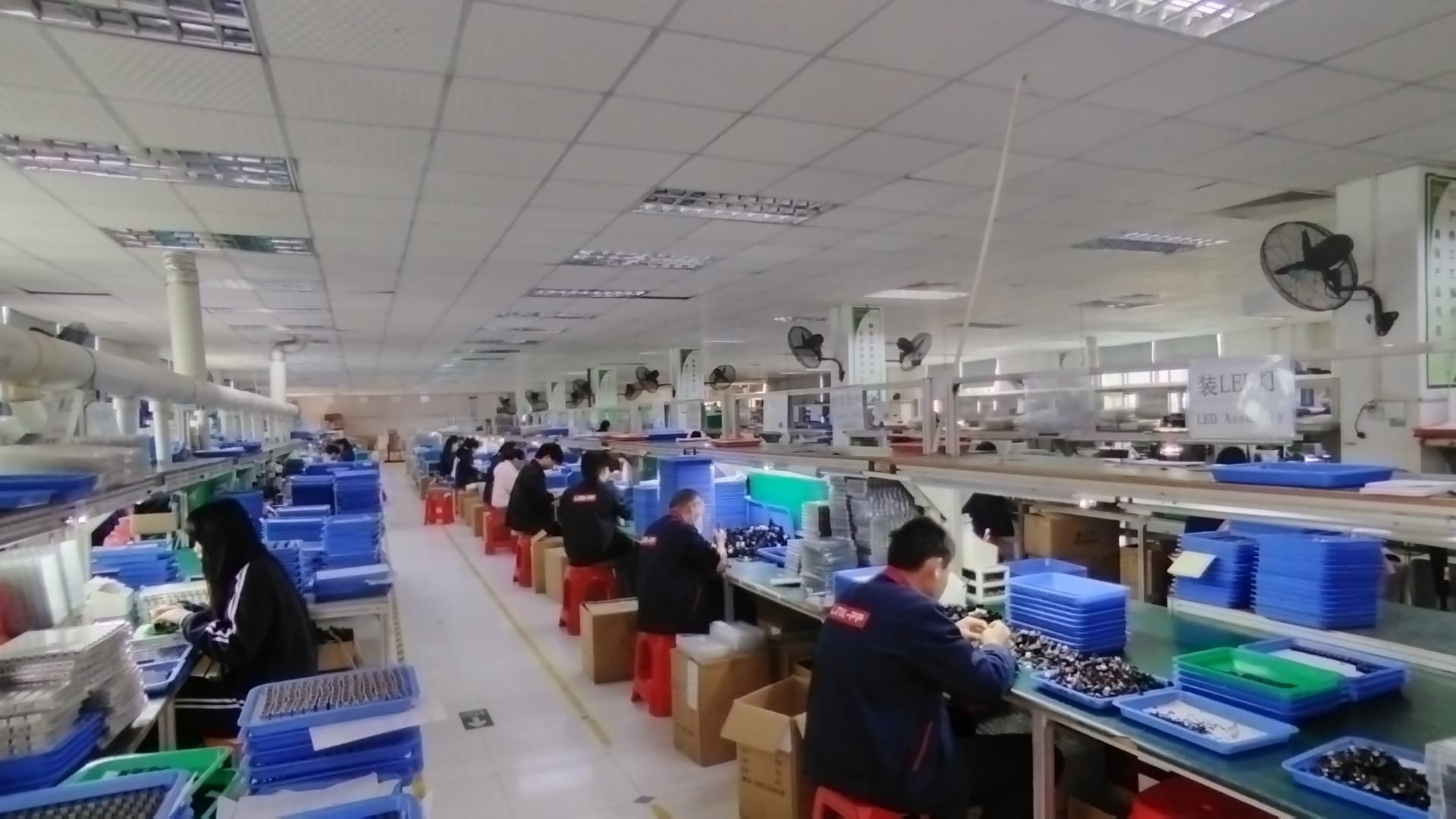
Furthermore, the integration of PCB manufacturing with nearby semiconductor packaging and assembly facilities allows for comprehensive solutions. For example, our memory modules benefit directly from this proximity. We source DRAM chips, design and optimize high-density PCB layouts, assemble, test, and ship complete products within a highly integrated geographic hub. This streamlined workflow reduces the overhead costs typically associated with multi-country sourcing models.
Real-world deployment of multi-layer PCBs and thermal systems across diverse environments.
Heavy-duty equipment like WIFI-enabled welding machines and high-voltage power inverters require multi-layer PCBs that handle high currents and control signal pathways without noise interference. Our multi-layer boards use heavy copper designs to ensure stable power delivery and system safety.
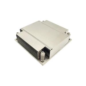
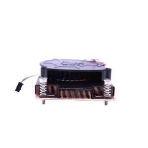
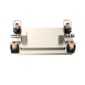
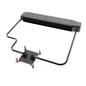
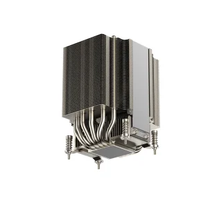
Modern data centers deploy dual-socket server platforms (such as LGA4677 and AM5 processors) that generate significant heat. Standard layouts fail under these conditions. Combining high-frequency PCBs with tailored liquid cooling blocks and copper-fin heat sinks maintains optimal operating temperatures for server processors.
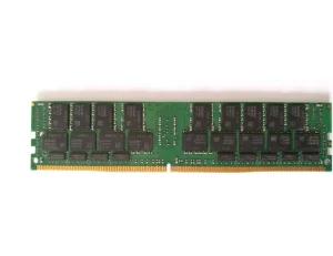
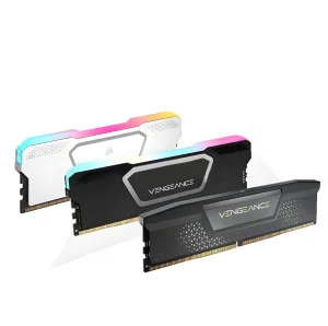
With DDR4 and DDR5 operating at high speeds (up to 6000MHz and beyond), signal paths must be highly optimized. Using low-loss PCB substrates, carefully matched trace lengths, and dedicated ground planes ensures stable performance and data integrity for gaming, industrial, and enterprise servers.
Navigating complex international certifications to ensure frictionless import and deployment.
Exporting complex hardware to major global markets (including North America, Europe, the Middle East, and Southeast Asia) requires strict adherence to international safety and environment standards. Kryntel ensures compliance at every stage of the manufacturing process:
We provide comprehensive support for our partners, offering custom packaging design, specialized firmware configuration, and electrical validation reports. Whether you are a system integrator in Germany, a distributor in the US, or a hardware developer in the UAE, our dedicated export support team manages international shipping requirements, customs declarations, and compliance documentation for a smooth delivery process.
A professional memory and high-performance hardware manufacturer serving global partners since 2016.
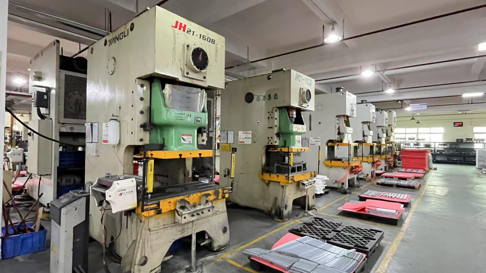
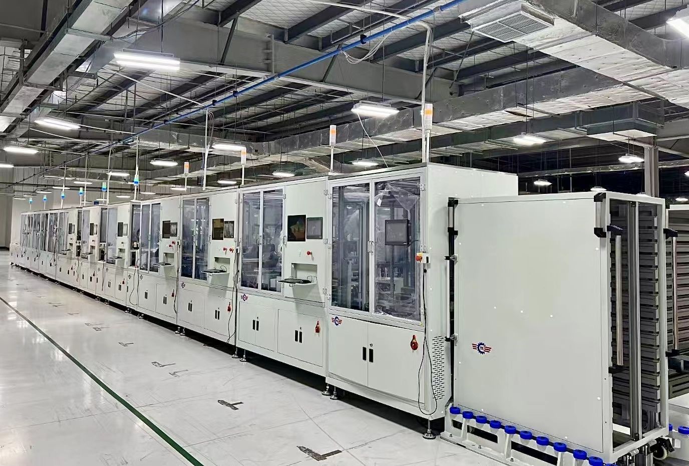
Founded in 2016, Kryntel Memory Technology (China) Co., Ltd. is a professional DDR5 memory manufacturer specializing in high-performance RAM modules for global OEM, ODM, and private label partners. With a modern production facility covering approximately 320㎡, we focus on delivering stable, high-speed, and energy-efficient memory solutions for gaming, industrial, and server applications.
Over the years, Kryntel has built strong export capabilities with annual export revenue ranging from USD 8 million to USD 18 million. The company has accumulated 6 years of export experience and 9 years of overall industry experience in memory and semiconductor-related manufacturing.
Our R&D department is highly capable, supporting advanced customization, including PCB design optimization, frequency tuning, heat dissipation solutions, and branding customization. We offer full OEM/ODM services with flexible customization options such as frequency, latency, heat spreader design, packaging, and firmware tuning.
In the past year, we successfully launched over 280 new memory products across DDR4 and DDR5 series. Our R&D team consists of approximately 160 engineers specializing in memory architecture, signal integrity, and product reliability optimization.
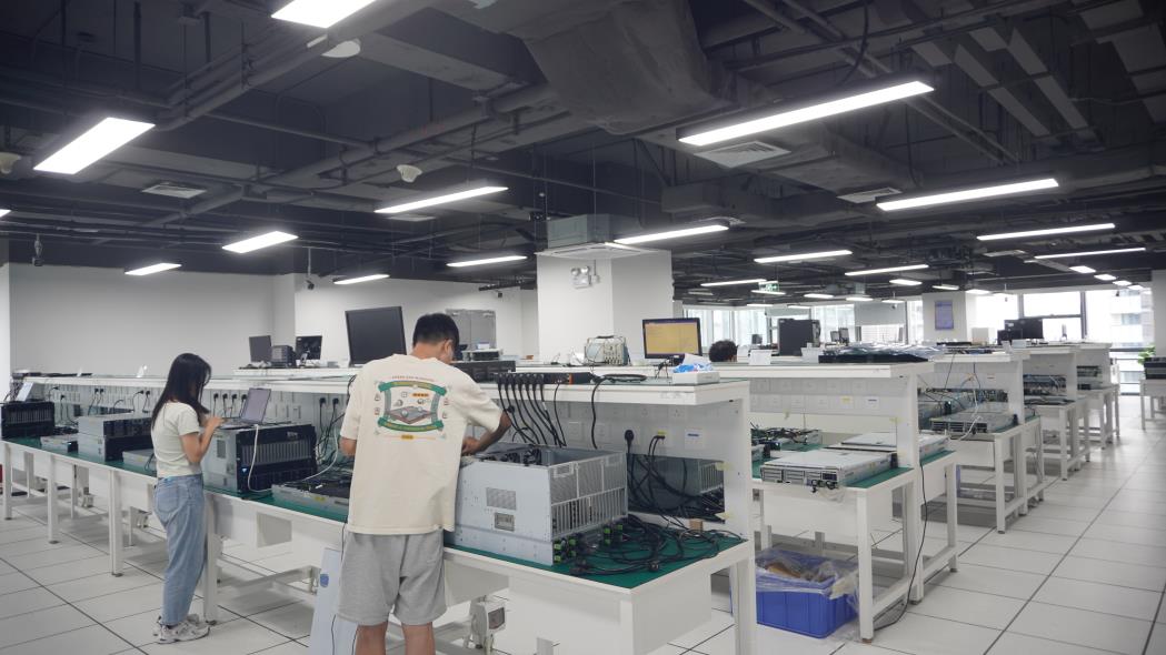
Our quality control system is built on strict multi-stage inspection standards, including incoming material inspection, in-process quality control, aging tests, and final product sampling inspection. Product testing methods include high-temperature aging tests, compatibility testing with major motherboard platforms, bandwidth stress testing, and voltage stability testing. We maintain a dedicated QA team of 42 professionals to ensure consistent product reliability.
Kryntel operates with a strong international trade background, supported by experienced export teams familiar with North America, Europe, the Middle East, and Southeast Asia markets. Our primary markets include the United States, Germany, India, Brazil, and the UAE.
We cooperate with a global supply chain network of approximately 1,200 upstream and downstream partners, ensuring stable sourcing of high-quality DRAM chips and components. Our main customer base includes computer hardware brands, system integrators, distributors, and e-commerce sellers.
Kryntel is committed to delivering cutting-edge memory solutions with consistent quality, competitive pricing, and long-term partnership value for global customers.


Answers to common engineering, quality management, and logistics questions from our global partners.
For standard 4 to 8-layer prototype PCBs, the typical lead time ranges from 3 to 5 working days. Large-scale volume production runs generally require 10 to 15 working days, depending on stack-up complexity, surface finish selections, and material availability. Special requirements, such as blind/buried vias or heavy copper layers, may adjust these timelines.
We use Polar Instruments software to design and simulate target impedances during layout preparation. Once manufactured, we measure and verify impedance tolerances (typically to within ±10%, or ±5% on demand) using Time Domain Reflectometry (TDR) test coupons on every panel, ensuring stable high-speed transmission.
Every production batch undergoes multi-phase testing, including high-temperature thermal stress aging, voltage sweep testing, and bandwidth stress tests. Compatibility is checked across major chipset platforms (Intel & AMD) using motherboards from leading manufacturers to ensure plug-and-play stability under load.
Yes, our engineering team offers full ODM and OEM customization. We support changes to PCB trace layouts, frequency settings, and EEPROM firmware configurations, alongside custom heatsinks, thermal spreaders, retail boxes, and bulk packaging styles.
We work with international logistics providers to offer reliable shipping options, including express air freight, sea freight, and combined rail cargo. Our dedicated logistics team prepares customs documents, HS code classification sheets, and certificate declarations to prevent customs delays.
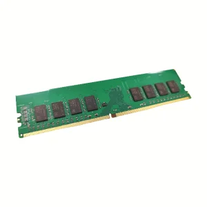
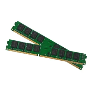
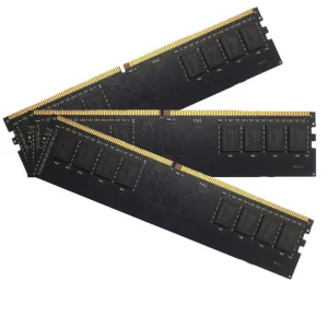
Explore our line of server radiators, desktop memory upgrades, and high-performance cooling components.
 Kryntel