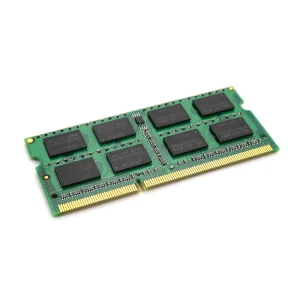
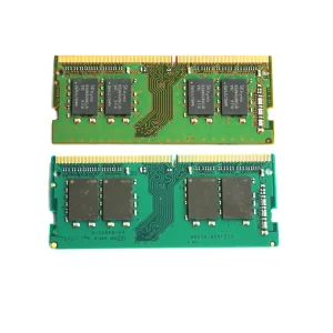
In the rapidly evolving world of electronics, Printed Circuit Boards (PCBs) form the foundational backbone of physical digital networks. As systems scale down in volume and scale up in functional complexity, selecting the appropriate board geometry—whether it is a classic single-sided PCB or a high-performance double-sided PCB—becomes a critical choice. Our manufacturing lines integrate advanced chemical copper deposition, state-of-the-art automated optical inspection (AOI), and precise mechanical drill rigs to deliver boards with unparalleled electrical reliability and structural durability.
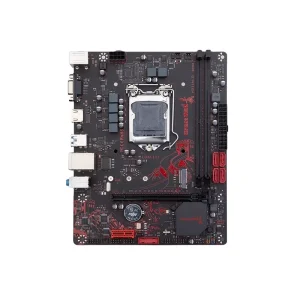
Double-sided PCBs utilize a structural core layer clad with copper on both the top and bottom faces, connected electrically via high-integrity Plated Through-Holes (PTH). This architecture allows for a higher component density and more complex signal routing, making it the industry benchmark for standard computer peripherals, industrial controls, and power delivery architectures.
Modern PCB layouts necessitate tight impedance control, high-Tg (glass transition temperature) thermal ratings, and minimum trace-width tolerances. By executing rigorous design-for-manufacturability (DFM) reviews on every incoming Gerber file, we guarantee that all single-sided and double-sided structures perform stably under harsh ambient environments.
Double-sided designs leverage critical crossovers that reduce EMI (Electromagnetic Interference), enable decoupling capacitor placements directly beneath active components, and double the structural density.
Understanding the exact physical limits of each configuration is paramount for hardware architects looking to balance manufacturing overhead with electrical efficacy.
| Feature / Metric | Single-Sided PCBs | Double-Sided PCBs | Industry Standard (IPC Class II/III) |
|---|---|---|---|
| Layer Count | 1 Layer (Single Copper Clad) | 2 Layers (Double Copper Clad) | 1 to 2 Layers (Rigid Core) |
| Routing Density | Low (No trace crossover allowed) | Medium to High (Using PTH Vias) | Varies based on trace spacing |
| Solder Mask Layers | 1 Layer (Bottom side) | 2 Layers (Top & Bottom) | Liquid Photoimageable (LPI) Solder Mask |
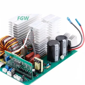
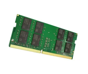
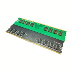
| Typical Applications | ZX7 welding machine motherboard, simple sensors | DDR4/DDR5 Memory, system controls, high-speed interfaces | High reliability computing & power electronics |
| Thermal Dissipation | Lower (Limited thermal routing options) | Superior (Utilizing thermal vias & metal cores) | Taconic TLY-5, Aluminum Backed, FR-4 High-Tg |
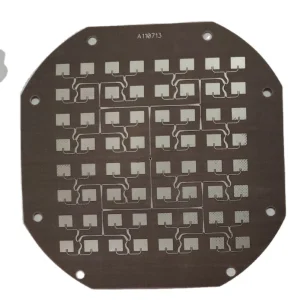
Our manufacturing facility sources raw copper laminates, prepregs, and exotic dielectrics from trusted global vendors. For high-frequency radio frequency (RF) circuits, we utilize high-frequency substrates such as Taconic TLY-5 (0.254mm) and advanced low-loss PTFE laminates. This guarantees that signal damping is minimized, and impedance calculations match real-world telemetry closely.
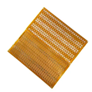
Whether you require heavy-copper (up to 6oz) structures for high-current power stages (like 220V ZX7 inverter motherboards) or thin, polyimide flexible layers (FPC) for space-constrained consumer designs, we provide tailored laminates optimized for your thermal profile.
Protecting exposed copper traces from oxidization is vital. We supply a range of surface finishes including Electroless Nickel Immersion Gold (ENIG), Hot Air Solder Leveling (HASL Lead-Free), and Organic Solderability Preservatives (OSP), each calibrated for automatic pick-and-place precision.
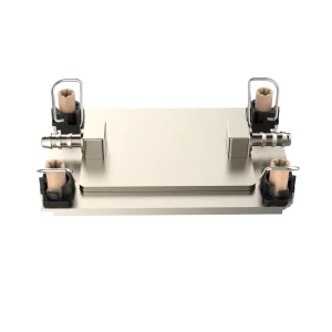
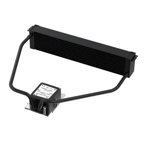
To prevent thermal stress fractures in solid-state computing environments, we integrate high-performance aluminum cores and custom liquid-cooling channels, including server processors utilizing SP5/LGA4677 heatsink blocks.
Founded in 2016, Kryntel Memory Technology (China) Co., Ltd. has expanded from a specialist DDR5 memory manufacturer into a powerhouse for global electronics OEM/ODM solutions.
With a state-of-the-art facility operating advanced assembly systems, we manage high-capacity productions alongside complex customization projects. Our specialized R&D division houses over 160 engineers dedicated to signal integrity, thermal dissipation, and PCB layout optimization.
Every batch undergoes a multi-layered testing regimen: flying probe testing, AOI (Automated Optical Inspection), X-ray solder integrity tests, thermal stress cycle chambers, and high-frequency vector network analysis. This ensures that every high-sensitivity PCBA, like those found in gold metal detectors, maintains zero field failure rates.
Procuring single-sided and double-sided PCBs from China provides unparalleled benefits. The dense manufacturing clustering in Guangdong and the Yangtze River Delta guarantees direct access to raw chemicals, copper clad laminates, and specialized chipsets with zero logisitical friction.
Integrated supply chains mean we can source rare dielectrics, Taconic materials, and specialized IC components within 24 hours, ensuring prototype turns can be completed in as little as 3 working days.
From adjusting trace layouts to resist high vibration profiles, to fabricating flexible keyboard matrices, our OEM/ODM pathways support rapid product scaling.
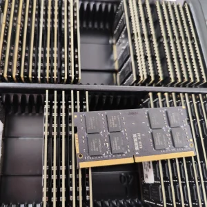
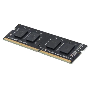
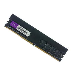
As a premier memory module factory, we integrate high-speed DDR4/DDR5 DRAM dies directly into processing boards, eliminating intermediate distribution costs.
We provide full-spectrum compliance certifications including UL, RoHS, and IPC Class III standards to meet rigorous European and North American industrial requirements.
Modern electronic assemblies must operate reliably across diverse and harsh environmental conditions. The engineering behind our single and double-sided PCBs is optimized to address unique challenges in specific vertical industries.
Heavy-duty machinery like inverter welders requires PCB designs that withstand sustained thermal shock and high power surges. Our 220V ZX7 motherboard series uses heavy copper layers (up to 3oz) and protective conformal coatings to prevent dielectric breakdown in dust-prone environments.
Modern thin-profile devices require flexible PCB integration. Our Polyimide FPC modules support micro-trace pitches down to 0.1mm, ensuring durability over millions of flex cycles in laptops and mechanical keyboard arrays.
Deploying high-frequency radar or signal receivers calls for specialized dielectrics. Utilizing Taconic TLY-5 substrates with a thickness of 0.254mm, we support low-attenuation high-speed RF designs ideal for industrial detectors and modern avionics.
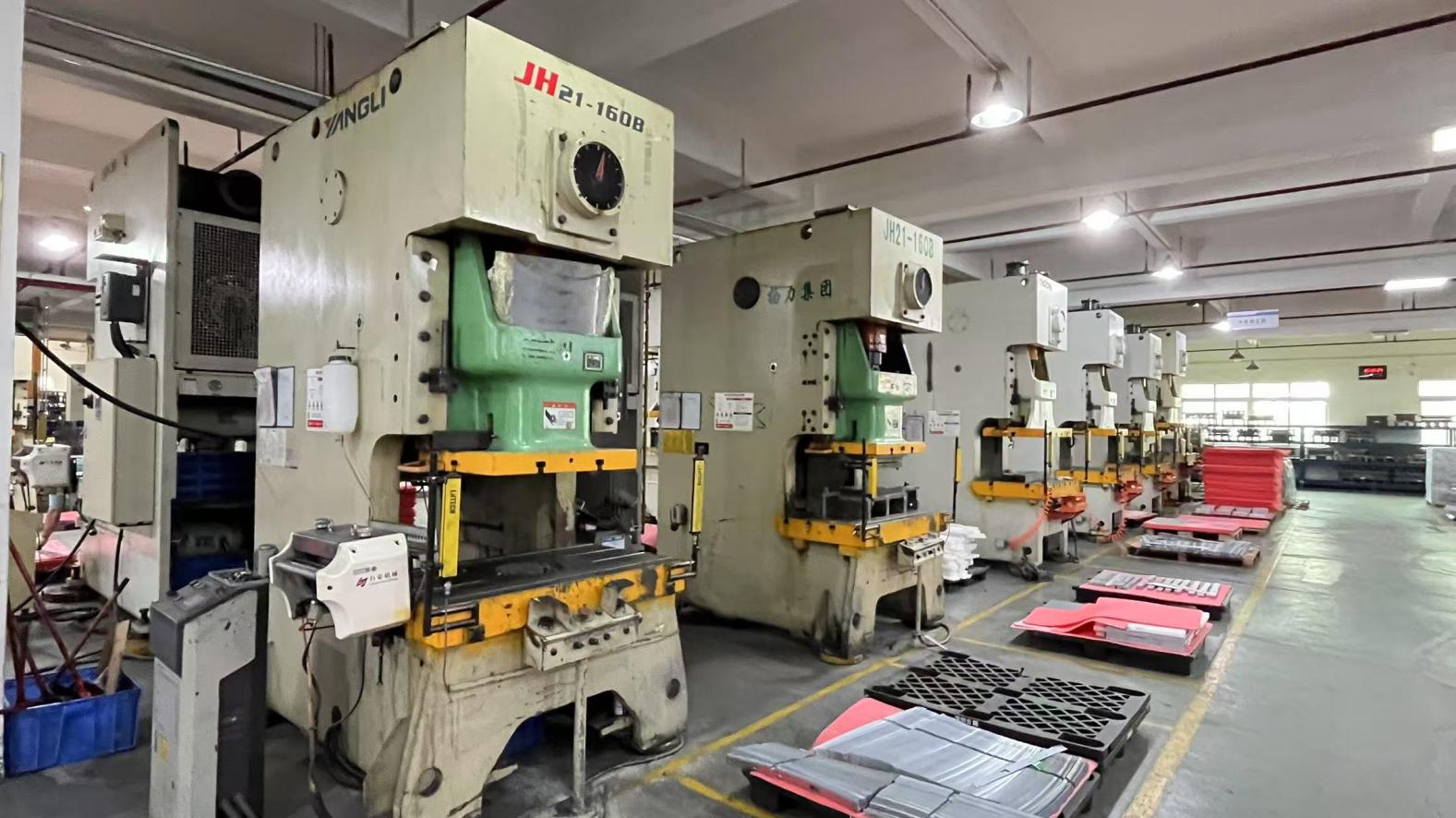
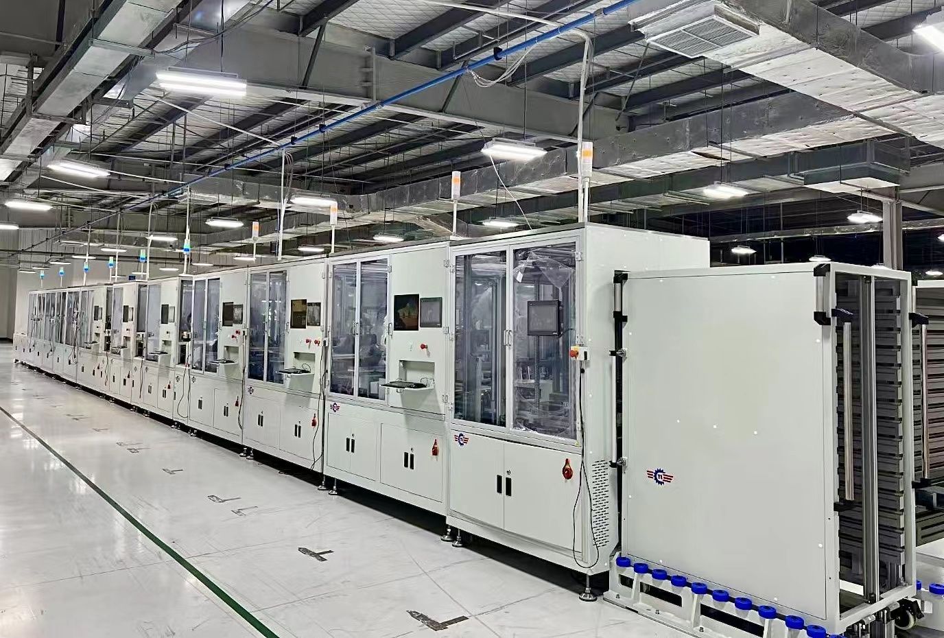
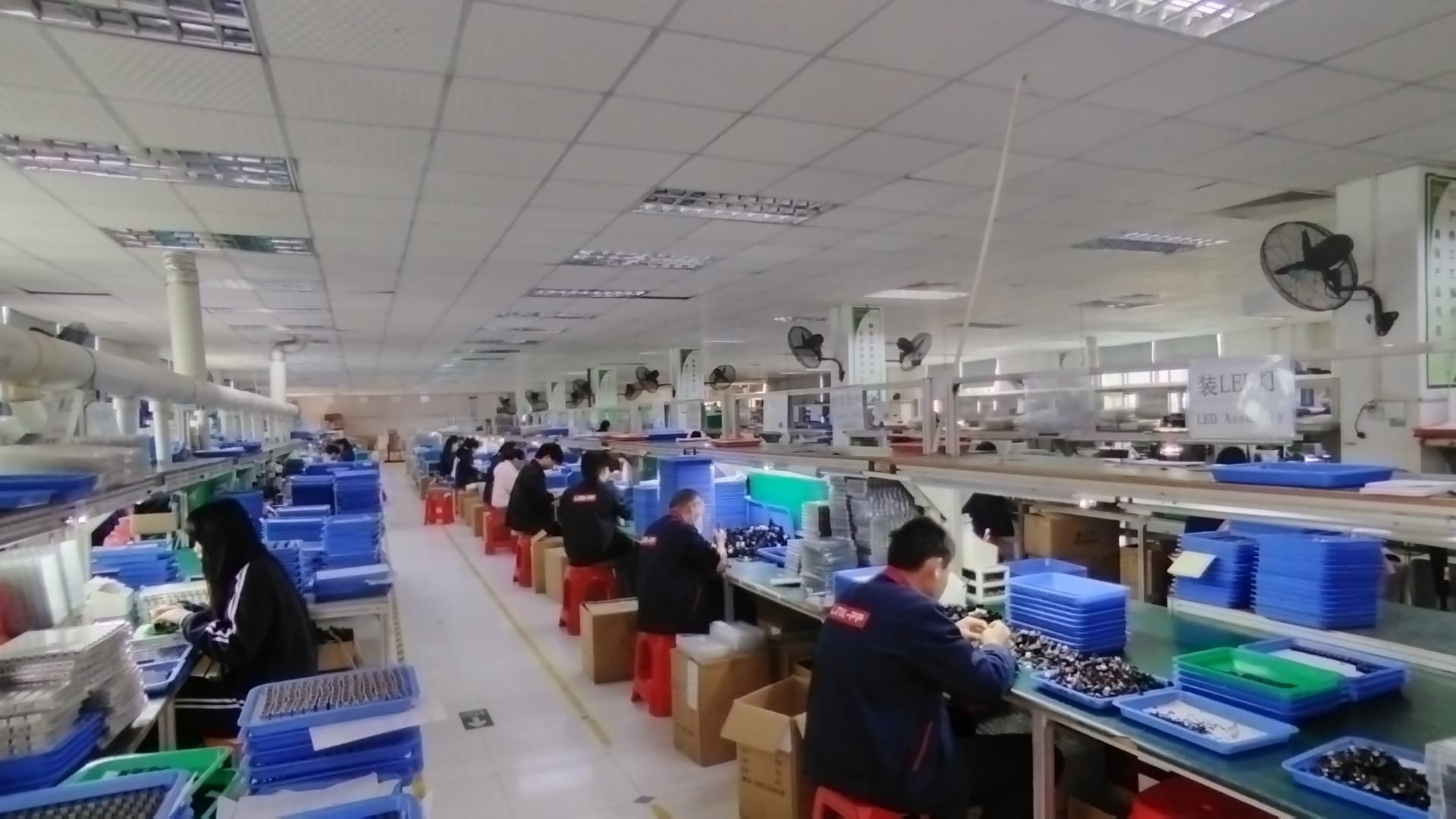
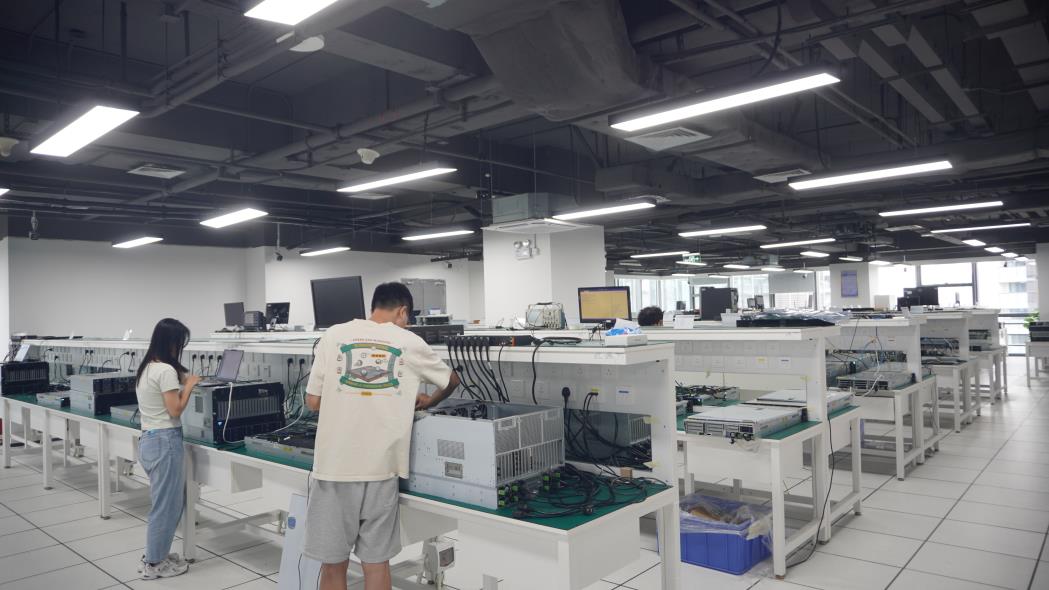
Take a look inside our cleanrooms, automated SMT lines, and quality verification centers where our engineers supervise the fabrication of memory modules, server cooling solutions, and custom PCBs.


Global sourcing agents, distributors, and computer brand owners require high supply security and short lead times. Kryntel mitigates market risks through advanced component forecasting and buffer inventory arrangements.
By maintaining deep relationships with major DRAM chip foundries, we offer robust allocations for DDR4 and DDR5 memory modules. Global enterprises can customize frequency profiles, thermal spreaders, packaging, and EEPROM settings to build custom product lines.
Our export distribution channels reach key industrial regions in Europe, North America, the UAE, and South America, ensuring seamless custom clearance and flexible incoterm agreements.
Find quick answers to common engineering questions regarding layout parameters, testing, and production capabilities.
 Kryntel