Engineered to support High-Density Power Electronics, Telecommunications, and Extreme Thermal Environments
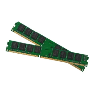
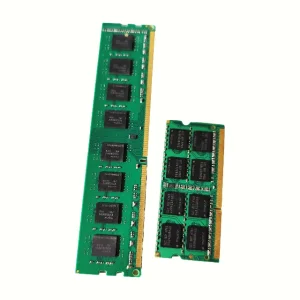
Unlocking the thermal and electrical performance thresholds demanded by Silicon Wadi’s pioneers.
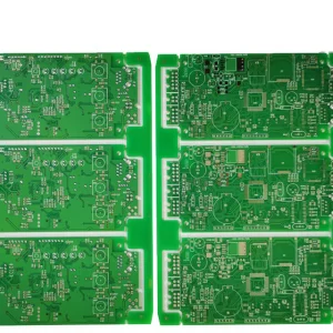
In the global arena of high-technology engineering, Israel stands as a powerhouse of R&D and hardware innovation. The local ecosystem—spanning Tel Aviv's tech startups, Haifa's R&D hubs, and national defense manufacturers—is built upon a relentless push for miniaturization, reliability, and power density. At the core of this engineering push is the requirement for advanced printed circuit boards capable of handling high-power distribution and extreme heat dissipation: Thick Copper PCBs (often classified as heavy copper PCBs with copper weights ranging from 3 oz/ft² up to 20 oz/ft²).
As a leading PCB and semiconductor-related manufacturer, Kryntel Memory Technology (China) Co., Ltd. bridge the gap between complex R&D design and high-volume, cost-effective production. By supplying robust multi-layer board stack-ups with heavy copper layers, we enable Israeli engineers to execute designs that operate under high electrical loads while maintaining low junction temperatures.
Enables high-current routing on inner and outer layers without excessive track widths.
Withstands harsh environmental testing profiles under MIL-PRF standards.
Direct integration of inductors and transformers into the board layers for space efficiency.
Paired with TG170/TG180 FR4 or polyimide matrices for continuous high-temperature performance.
Your Trusted Manufacturing & Global Supply Chain Partner
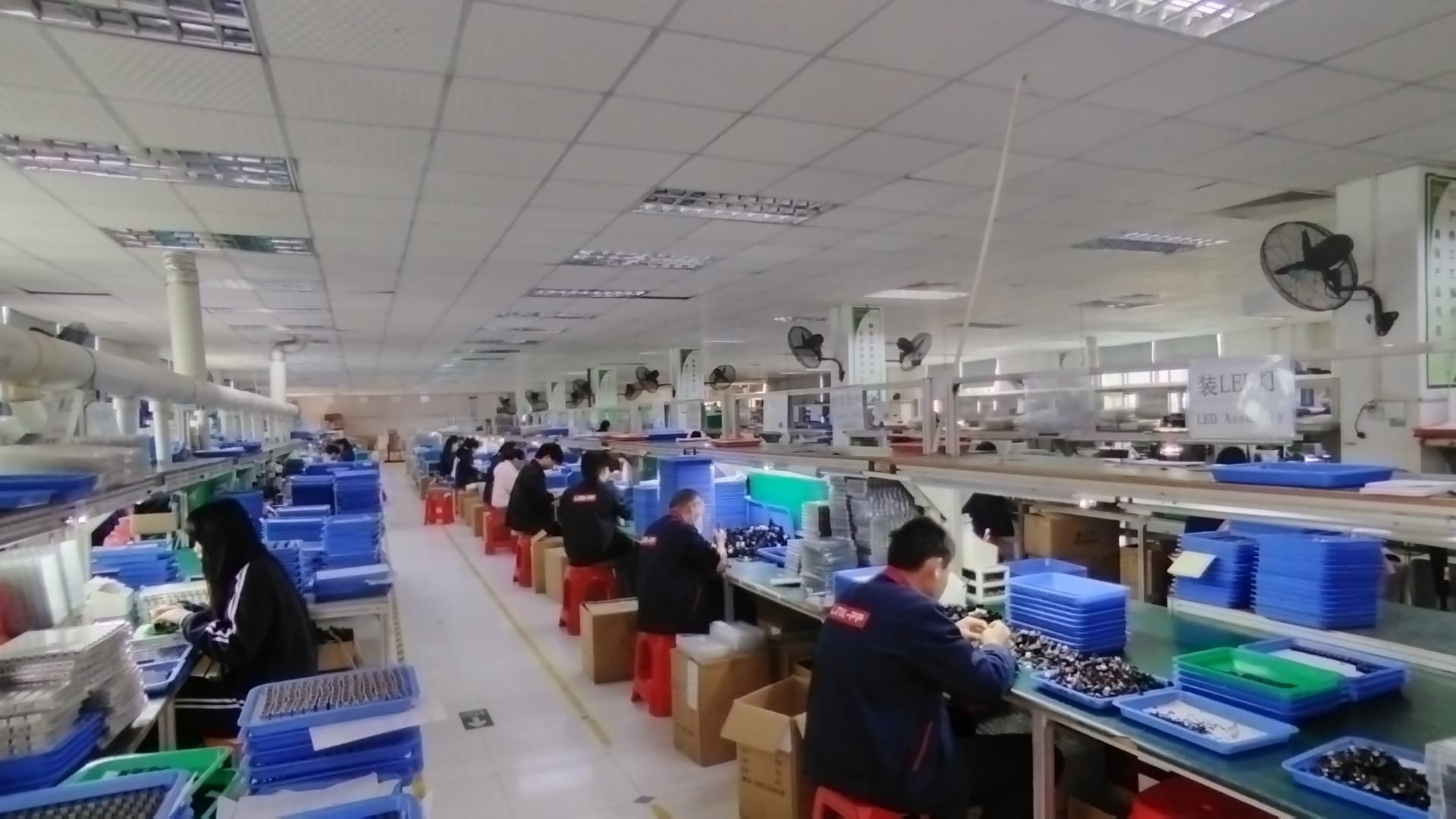
Founded in 2016, Kryntel Memory Technology (China) Co., Ltd. is a professional memory and hardware solutions manufacturer specializing in high-performance modules and circuit boards for global OEM, ODM, and private label partners. With a modern, highly optimized production facility covering approximately 320m², we focus on delivering stable, high-speed, and energy-efficient systems for gaming, industrial, aerospace, and server applications.
Over the years, Kryntel has built robust export capabilities with annual export revenue ranging from USD 8 million to USD 18 million. Having accumulated 6 years of export experience and 9 years of overall industry experience in memory and semiconductor-related manufacturing, we understand the specific quality controls required to pass rigid international evaluations.
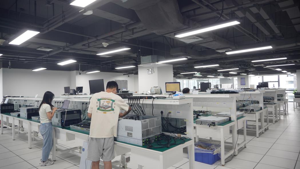
Our quality control system is built on strict multi-stage inspection standards, including incoming material inspection, in-process quality control, aging tests, and final product sampling inspection. Product testing methods include high-temperature aging tests, compatibility testing with major motherboard platforms, bandwidth stress testing, and voltage stability testing. We maintain a dedicated QA team of 42 professionals to ensure consistent product reliability.
Supported by experienced export teams familiar with North America, Europe, the Middle East (specifically Israel), and Southeast Asia, our primary markets include the United States, Germany, India, Brazil, the UAE, and Israel. We cooperate with a global supply chain network of approximately 1,200 upstream and downstream partners, ensuring stable sourcing of high-quality DRAM chips, heavy copper clad laminates, and advanced chemistry components. Our primary customer base includes computer hardware brands, system integrators, telecom distributors, and e-commerce sellers.
A guide for Israeli power design engineers when specifying heavy copper trace geometries.
In aerospace, military (e.g., radar, UAV control systems), and energy grids in Israel, thermal performance is paramount. Standard IPC-2221 calculations for track width vs. current carrying capacity change drastically when designing with heavy copper. A trace that would require a width of 100mm on 1 oz copper to carry 50A safely can be reduced to just 10mm when utilizing a 10 oz copper plane, allowing for highly compact system footprints.
Furthermore, our engineering teams optimize the stack-up by integrating resin-filling processes. Due to the high height of heavy copper traces, standard prepreg cannot completely fill the gaps, leaving voids that lead to localized breakdown under high voltages. Kryntel uses vacuum-pressed high-flow resin systems to eliminate these micro-voids, ensuring long-term dielectric reliability.
Understanding supply chain resilience, cost amortization, and customization standards.
In recent years, the global hardware electronics market has shifted toward localized R&D but centralized, high-efficiency manufacturing. Silicon Wadi engineers demand fast turnaround times for prototypes, followed by smooth scaling into volume production. However, raw material price fluctuations (specifically LME copper indices) and logistics blockages pose threats to system integrators.
How We Address Global Procurement Bottlenecks:
This macro approach ensures that our customers in Tel Aviv, Haifa, or Beer Sheva receive the exact technical specifications they need without suffering from the standard 6-to-8 week delays common in unoptimized supply chains.
Multi-stage inspection protocols ensuring zero-defect rates for global shipments.
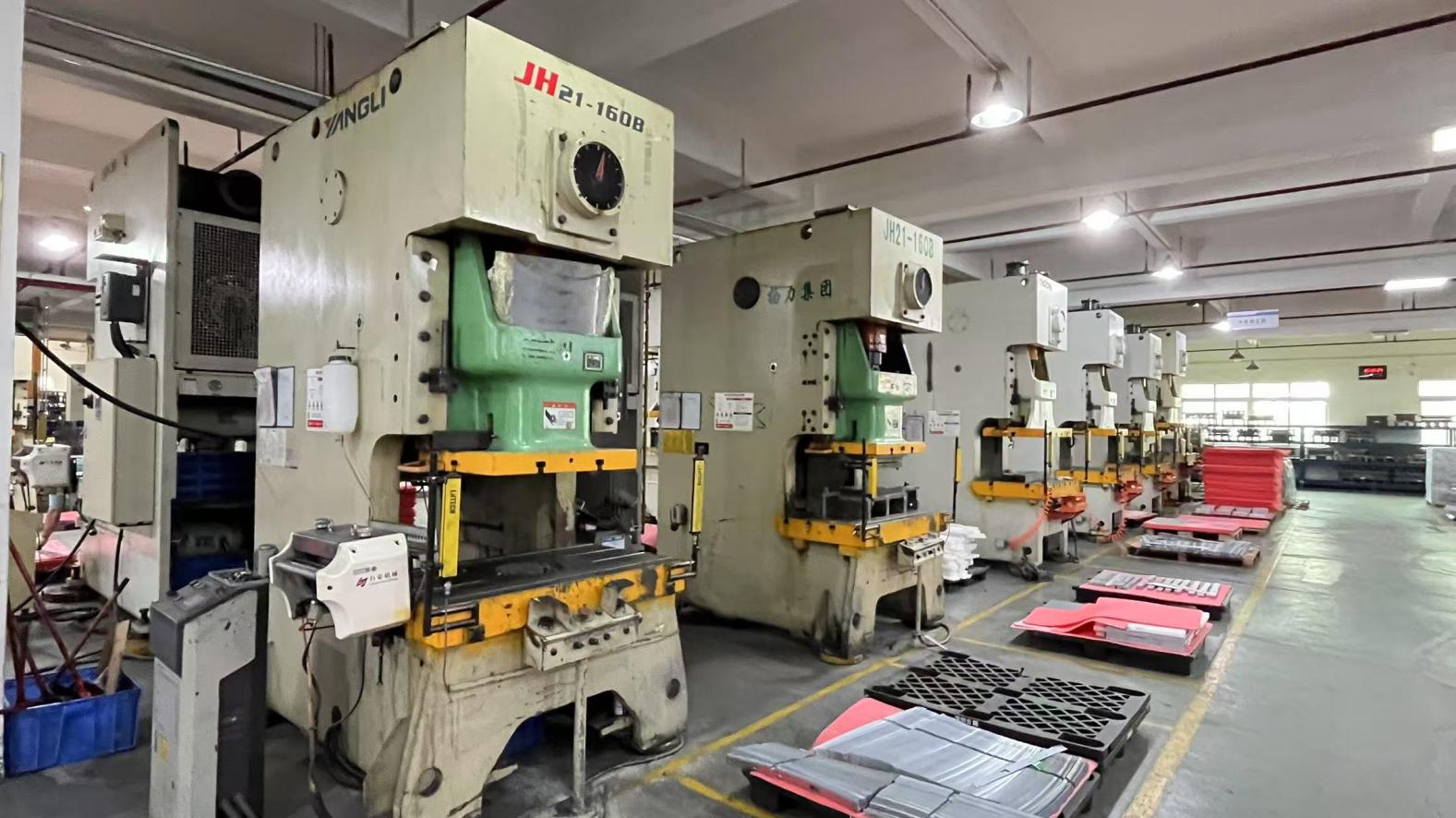
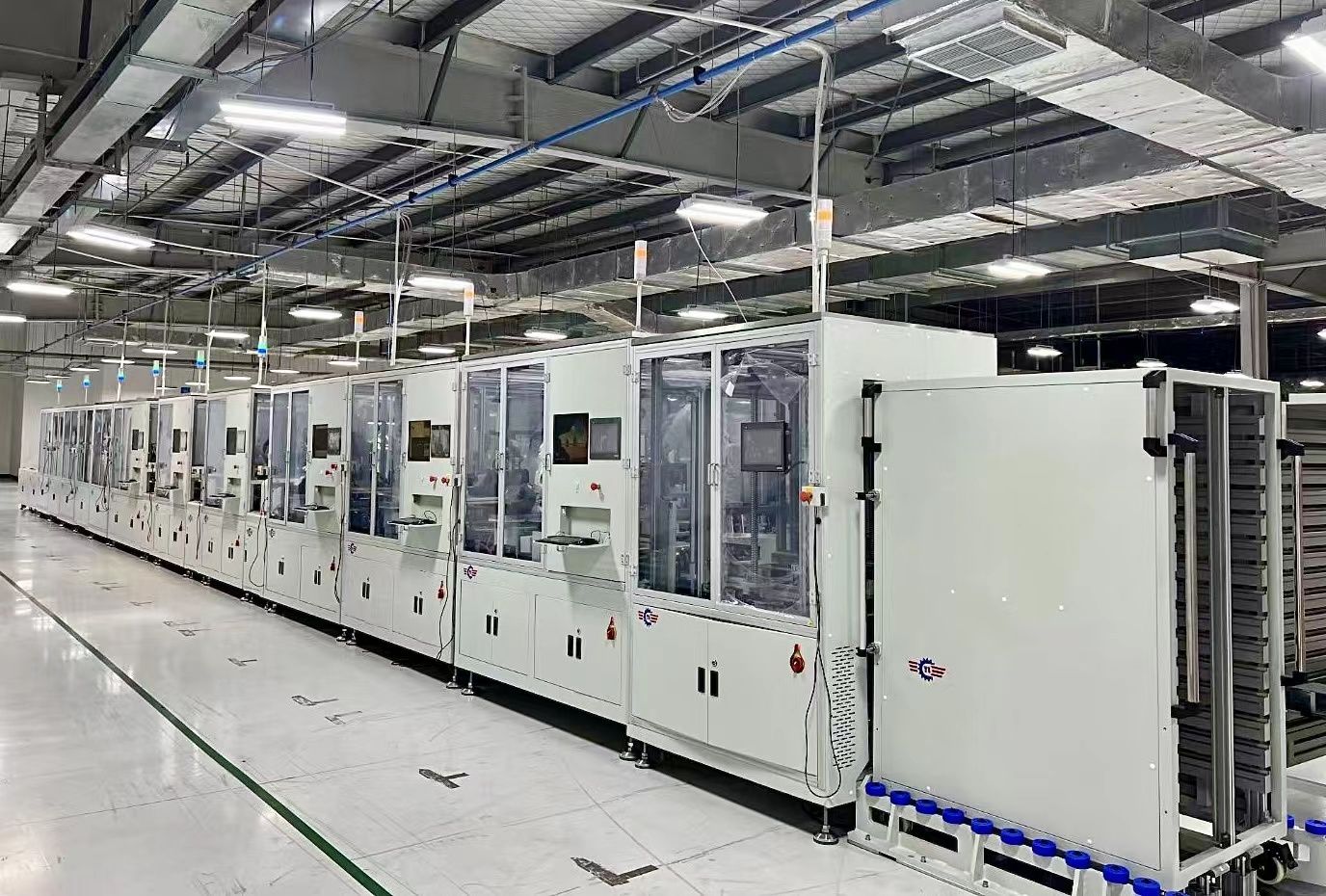


How power-delivery networks and high-frequency memory modules intersect.
In high-performance computing (HPC) nodes, artificial intelligence clusters, and military processing units, raw compute power must be matched with efficient heat dissipation and electrical stability. A server motherboard utilizing an Intel LGA4677 or AMD socket architecture demands complex power delivery networks (PDN). Thick copper layers within these motherboards are essential for regulating transient currents and mitigating voltage drops under maximum workloads.
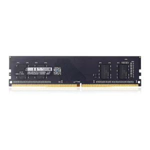
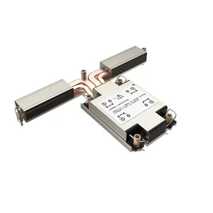
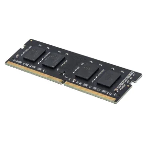
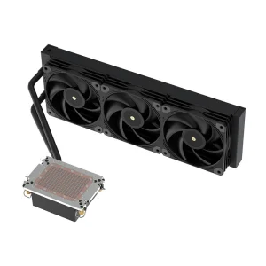
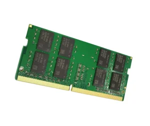
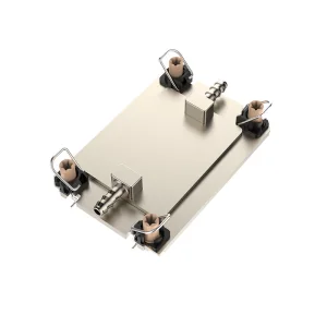
As a manufacturer deeply integrated into both PCB production and DDR4/DDR5 memory modules, Kryntel has a unique advantage. We analyze the board layout from a systems level. Our engineers design memory modules to interface seamlessly with thick copper backplanes and server architectures, preventing impedance mismatches and optimizing thermal transfer toward passive extruded radiators or water cooler blocks.
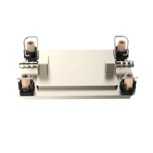
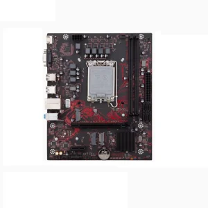
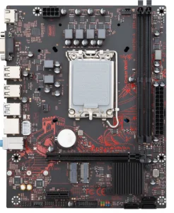
Whether you are implementing an industrial motherboard compatible with LGA1700 or designing high-capacity server arrays, integrating thermal components like 400W water cooling blocks directly onto heavy copper substrates ensures optimal device lifetimes and stable operational margins.
Adhering to strict international standards for aerospace, medical, and defense systems.
Answers to engineering and supply questions about Thick Copper PCBs.
Full suite of memory modules, motherboards, and server cooling accessories for industrial systems.
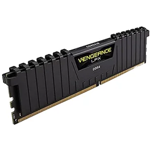
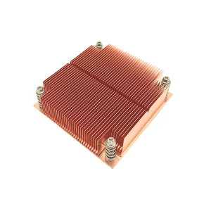
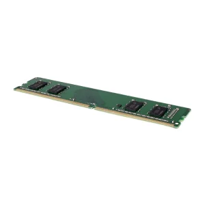
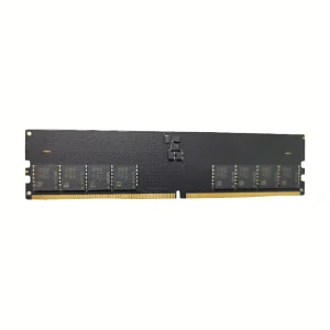
Looking to deploy heavy copper substrates or memory customizations in your next aerospace, energy, or industrial compute application? Let our team of DFM specialists review your specifications.
Send Inquiry Now Kryntel