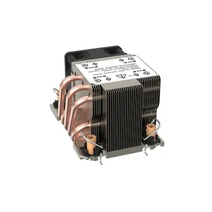
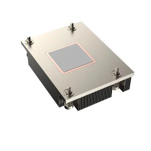
Pioneering multi-layer designs engineered to meet structural, integrity, and thermal requirements of Boston's elite tech firms.

The Greater Boston metropolitan area, anchored by Cambridge's Kendall Square and the historic Route 128 technology corridor, represents one of the most critical technology hubs globally. The demand for electronic components here differs significantly from consumer-grade markets. Industries like robotics, biotechnology, and high-performance computing (HPC) require ultra-reliable, high-signal-integrity, and highly complex multi-layer printed circuit boards.
Whether it is deep-submersible robotics, custom medical sensor arrays, or multi-phase high-frequency power controllers for high-performance servers, Boston engineers work with tight tolerances. Standard consumer-grade PCBs fail under these demands. They require high-density interconnect (HDI) technologies, microvias, and low-loss substrates to handle gigabit speeds with low signal degradation.
As layers increase beyond 4 to 6 layers, and up to 32 layers, managing parasitic capacitance, loop inductance, and impedance mismatching becomes critical. In Boston's scientific and engineering sector, high-frequency design requires precise material and structural specifications:
Substrate Choice: Standard FR-4 is often insufficient for gigahertz-range signaling. For low-loss, high-speed applications, we manufacture utilizing advanced materials like Rogers, Isola, and Megtron to maintain minimal dissipation factors (Df) and dielectric constants (Dk).
Microvia Geometry: Stacking or staggering blind and buried microvias allows for high routing density without causing signal reflection. Lasers drill these microvias, which are then filled with copper plating to ensure reliable vertical connections across multiple dielectric layers.
With high-speed digital lines running parallel near high-power supply planes, mutual inductance poses a constant risk. Our layout guidelines incorporate solid reference ground planes directly adjacent to critical routing layers. This layout provides a direct return path for currents, shielding sensitive trace lanes from high-frequency electromagnetic noise.
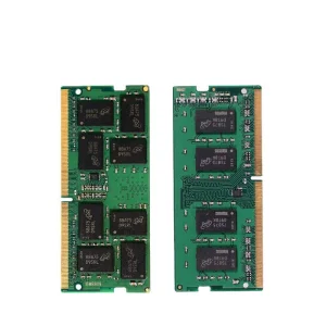
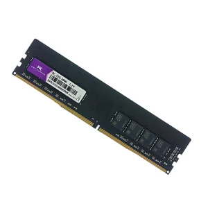
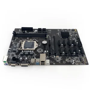
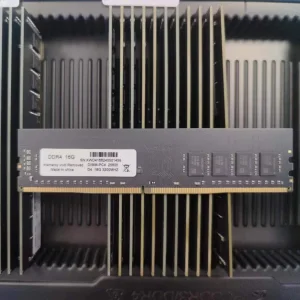
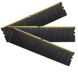
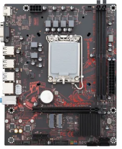
Explore our line of server-grade modules, industrial motherboards, and memory configurations designed for heavy workloads.
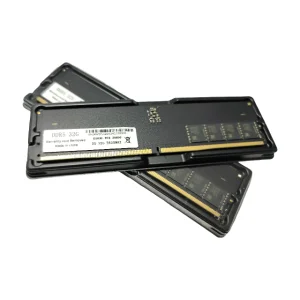
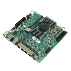
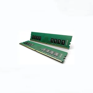
For Boston-based hardware companies, the speed of hardware iteration is critical. Building a functional prototype, testing it, and modifying it within a sprint cycle determines time-to-market. Historically, domestic fabrication options inside the US have faced constraints in production capacity, layering capability, or pricing. Utilizing a vetted, high-quality partner in China like Kryntel Memory Technology (China) Co., Ltd. resolves these constraints.
Working with an international factory requires robust logistical planning and communication. We maintain close partnerships with major carriers to schedule direct air transport routes from Shenzhen and Hong Kong to Boston Logan International Airport (BOS). This logistics pathway ensures that multi-layer prototypes transition from fabrication lines to assembly facilities in New England in as little as 3 to 5 business days.
Furthermore, our supply network integrates over 1,200 upstream and downstream partners. This deep industrial network ensures stable pricing and component availability even during global supply chain fluctuations. By securing DRAM dies, high-end laminates, and specialized microcontrollers in volume, we shield our clients from localized parts shortages and unexpected cost hikes.
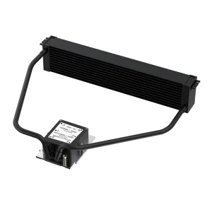
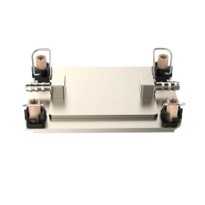
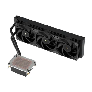
Ensuring power delivery, low latency memory processing, and active thermal cooling for complex industrial applications.
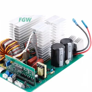
Founded in 2016, Kryntel Memory Technology (China) Co., Ltd. is a professional DDR5 memory and multi-layer hardware manufacturer specializing in high-performance memory modules and related hardware platforms for global OEM, ODM, and private label partners. In our modern production facilities, we focus on delivering stable, high-speed, and energy-efficient component solutions for industrial computing, medical electronics, and cloud server applications.
Over the years, Kryntel has built strong export operations, generating annual export revenues ranging from USD 8 million to USD 18 million. With 6 years of export experience and 9 years of overall industry experience in memory and semiconductor-related manufacturing, we align closely with Western engineering requirements, especially within critical engineering zones like Boston and Cambridge.
Our quality control system relies on strict multi-stage inspection standards, including incoming material inspection (IQC), in-process quality control (IPQC), thermal stress chamber tests, and final product sampling inspection (QA). Product testing methods include:
We maintain a dedicated QA team of 42 professionals to ensure consistent product reliability.
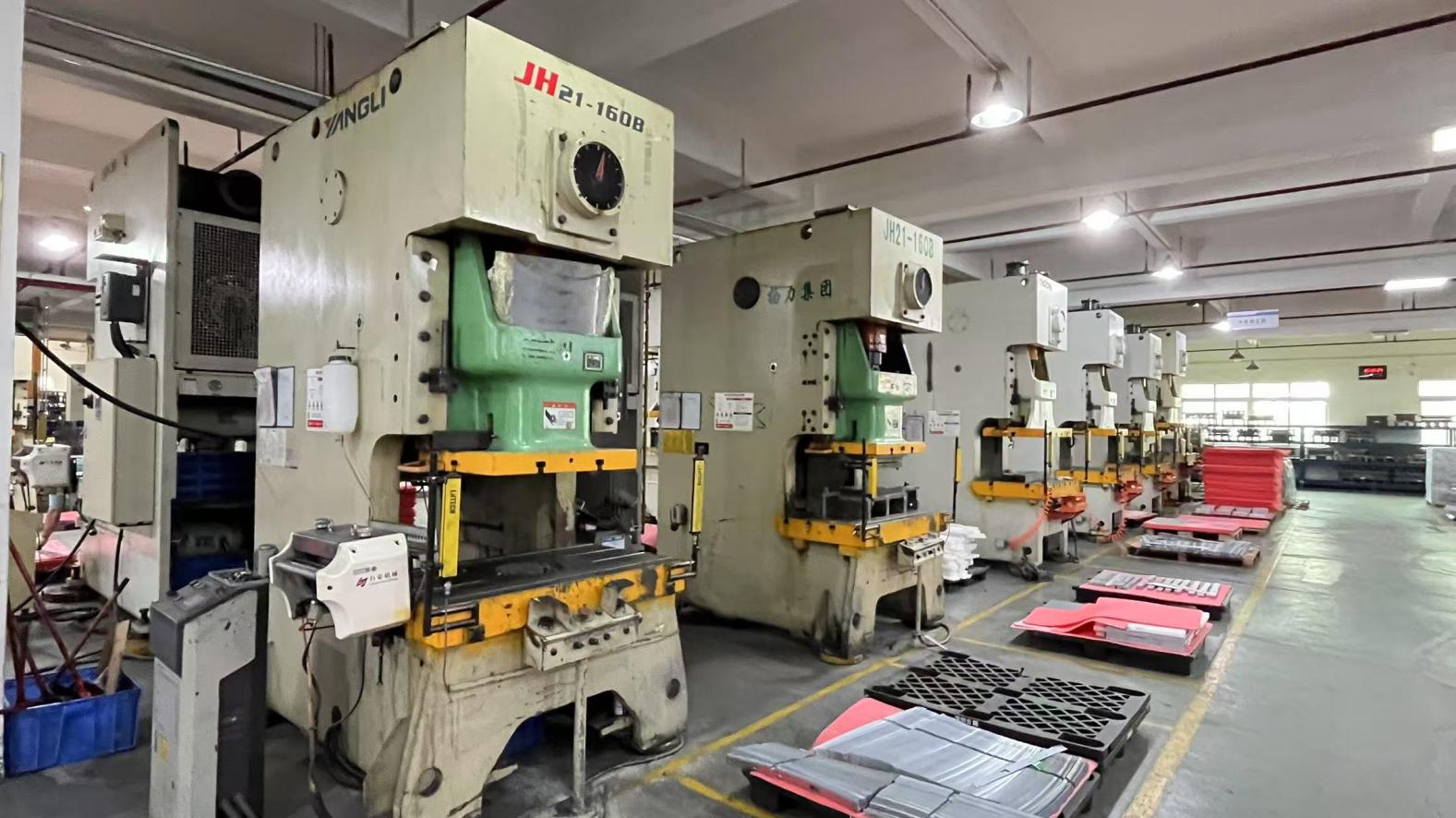
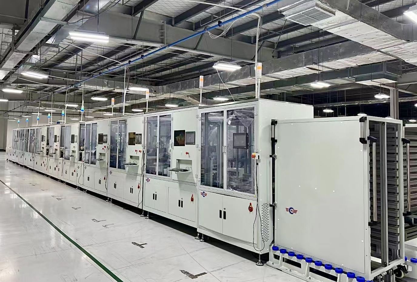
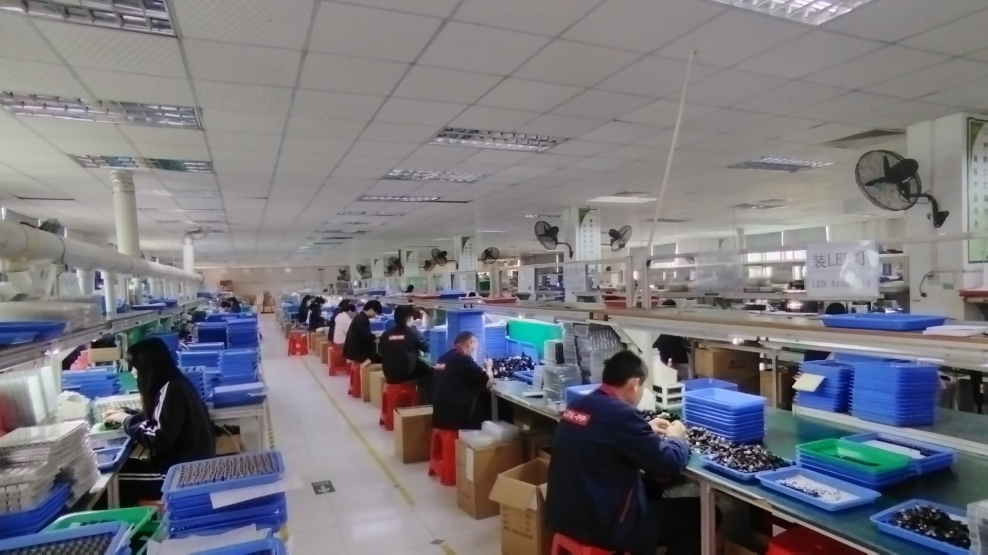
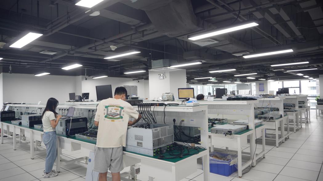
Inside the production, packaging, and high-temperature testing laboratories of Kryntel.


Expert technical insights regarding layout design, logistics, quality compliance, and hardware integration.
Get in touch with our engineering team to discuss your multi-layer PCB design, request a quote, or schedule a technical review.
 Kryntel