Explore our high-performance electronic assemblies and components compatible with Sweden's demanding manufacturing standards.
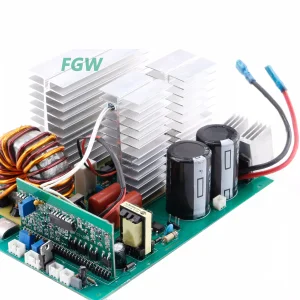
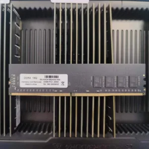
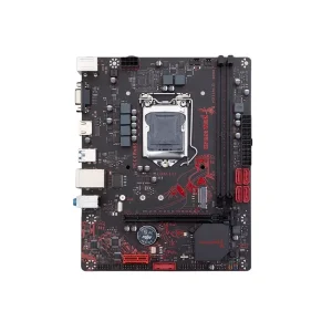
Sweden has long been a pioneer in the European electronics industry. Driven by giants in telecommunications (such as Ericsson in Stockholm's Kista Science City), automotive technology (such as Volvo and Polestar in Gothenburg), and industrial automation (ABB in Västerås), the Swedish market requires highly reliable Electronics Manufacturing Services (EMS). The reliability of SMT (Surface Mount Technology) assembly on PCBs starts at the very first step: solder paste stencil printing.
As components shrink from 0402 and 0201 packages down to ultra-fine-pitch 01005 passives, WLCSP, and 0.3mm BGA assemblies, traditional etched stencils fail to provide the stencil aperture wall smoothness required. Modern Swedish SMT production plants depend on specialized laser-cut stainless steel stencils. Features like electropolishing, advanced nano-coating, and multi-level step-stencils have transitioned from high-end options to standard process requirements across Stockholm, Malmö, and Gothenburg's advanced manufacturing hubs.
Kryntel Memory Technology (China) Co., Ltd. addresses this demand by pairing micro-aperture laser cutting precision with state-of-the-art SMT capabilities, supporting custom production lines for high-mix, low-volume (HMLV) medical tech in Uppsala as well as high-volume automotive runs.
Leveraging LPKF stencil laser systems with a focused spot size down to 20µm, allowing extreme contour precision of ±2µm for ultra-dense PCBA layouts.
All stencils are engineered and fabricated to align with IPC-7525B design guidelines, optimizing the critical area ratio and aspect ratio for zero defect printing.
Tailored stencil coatings and metallurgy designed to counteract electrostatic and humidity fluctuations within Nordic electronic manufacturing facilities.
Understanding the engineering behind solder paste release efficiency, step thickness transitions, and micro-aperture geometry.
To achieve high first-pass yield in SMT lines, stencils must release solder paste cleanly. The transfer efficiency is heavily influenced by the stencil's metallurgy, aperture wall roughness, and nano-treatment coatings. Here is the comparative matrix of the materials we process and deliver to Swedish factories:
| Stencil Type | Material Base | Aperture Cut Quality | Typical Thickness (µm) | Primary Use Cases in Sweden |
|---|---|---|---|---|
| Fine-Grain (FG) Stainless Steel | Premium Fe-Cr-Ni fine-grain structure (1-2µm grain size) | Ultra-smooth sidewalls, low burr | 80 - 150 µm | Automotive PCBs, Smart grid electronics, medical devices. |
| Hydrophobic Nano-Coated Stencil | FG Steel + Molecular Fluoropolymer coating | Zero paste adhesion on aperture walls and bottom side | 60 - 120 µm | 01005 passives, 0.3mm Pitch BGA, WLCSP, dense consumer electronics. |
| Multi-Level Step-Stencil | SUS304 or FG Steel (precision milled or dual etched) | Varying heights for high and low volume deposits | 60 to 250 µm locally on a single sheet | Mixed technology boards combining shielding cans/connectors with fine-pitch BGAs. |
| Electroformed (E-Form) Nickel Stencil | Pure Nickel additive electro-deposition | Atomically smooth, tapered aperture walls | 50 - 100 µm | High-density semiconductor packaging, flip-chip SMT. |
At our engineering facility, we run comprehensive Design for Manufacturability (DFM) verification on incoming Gerber files from Sweden. We check two primary ratios:
If these criteria are not met, we recommend local step-down stencils or suggest adjusting the paste release area. When Swedish clients request PCB assembly solutions, this structural validation is performed systematically before physical laser cutting begins.
Maximizing efficiency, sourcing resilience, and providing fast logistics from Shenzhen directly to Swedish SMT facilities.
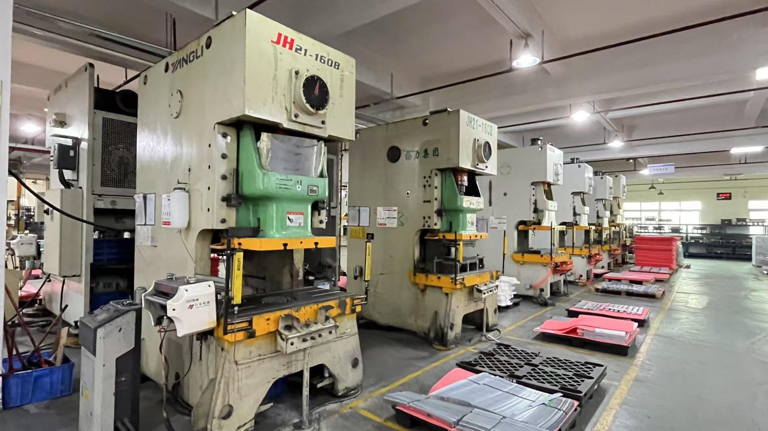
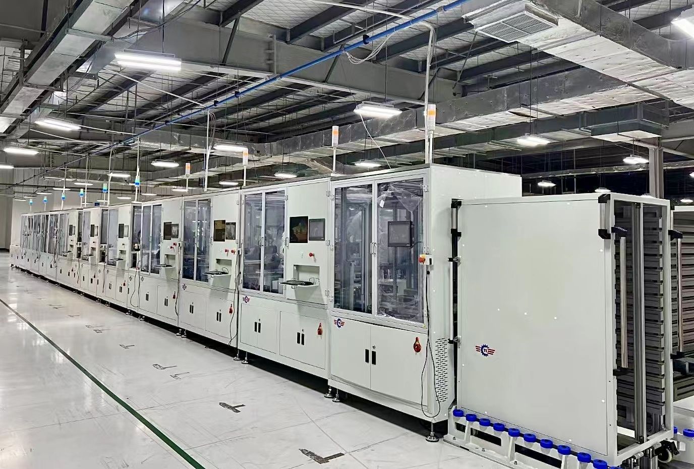
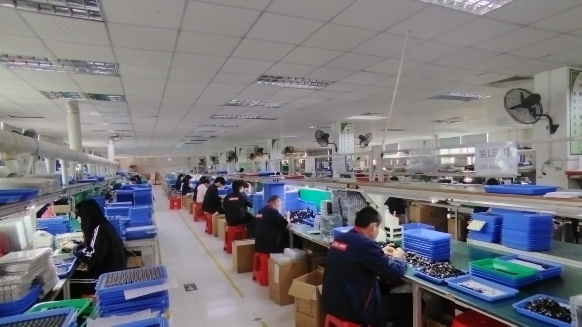
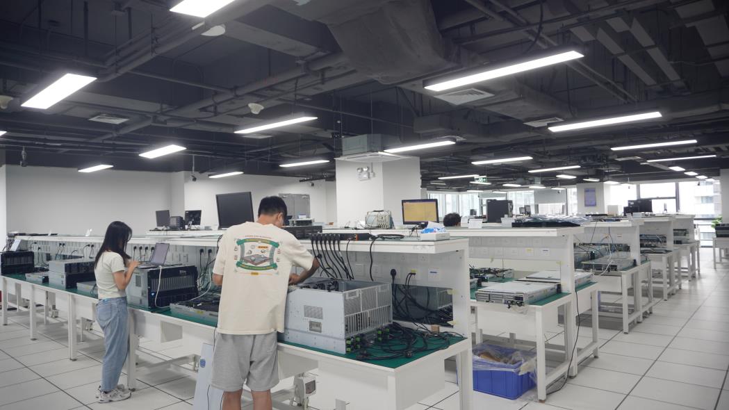
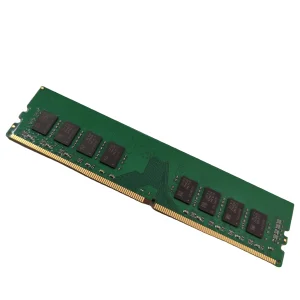
Kryntel Memory Technology (China) Co., Ltd. operates an advanced manufacturing system. While we are a leading manufacturer of DDR5 and DDR4 memory modules, our capability extends across high-precision PCB assembly (SMT/DIP) and OEM electronics fabrication. Our integrated supply chain offers significant competitive advantages for Swedish partners:
With annual export revenue ranging between USD 8 million to USD 18 million, our financial stability ensures secure capital for manufacturing, materials purchasing, and advanced laser technology acquisitions.
We meet strict EU standards to align seamlessly with Swedish corporate governance and environmental directives.
All stencils, coatings, components, and solder materials are lead-free and conform to the strict registration, evaluation, and restriction of chemicals under EU directives.
We perform deep-level audits of our metal sources, ensuring that tin, tungsten, tantalum, and gold (3TG) elements are sourced from conflict-free certified smelters.
We provide Delivered Duty Paid (DDP) options, letting our partners avoid handling import tariffs, VAT declarations, or customs delays in Sweden.


Detailed answers to critical technical questions asked by hardware engineers and purchasing managers in the Nordic market.
Fine-Grain (FG) stainless steel has a grain size of 1-2 microns, compared to 10-15 microns in standard SUS304. During laser cutting, the laser vaporizes the metal along grain boundaries. The smaller grain structure of FG steel results in significantly smoother aperture walls, reducing solder paste friction. This increases transfer efficiency by up to 15%, making it critical for fine-pitch components like 01005s and 0.4mm BGAs.
Step-stencils are used when a PCB combines fine-pitch components (which require minimal solder paste) with large connectors or power devices (which require high volumes of solder paste). A step-down stencil reduces thickness locally (e.g., from 120µm to 80µm) around fine-pitch QFNs to prevent bridging. A step-up stencil increases thickness locally (e.g., from 120µm to 180µm) to deposit sufficient paste for power electronics.
Hydrophobic and oleophobic nano-coatings are applied in a molecular layer (typically 2-4nm thick) to the bottom side of the stencil and inside the aperture walls. This prevents solder flux from wetting and spreading across the stencil underside. In production, this reduces under-stencil cleaning frequency from once every 3-5 prints to once every 25-30 prints. This minimizes solvent consumption, limits paper waste, and increases overall SMT printer uptime.
Our engineering team performs a full DFM analysis on Gerber RS-274X or ODB++ formats. Files are processed on standalone secure local networks. We sign strict Non-Disclosure Agreements (NDAs) with all Swedish partners and adhere to GDPR compliance protocols for data handling and secure file transfer.
OEM-grade, quality-tested semiconductor solutions and assembly services for international distribution.
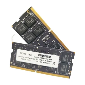
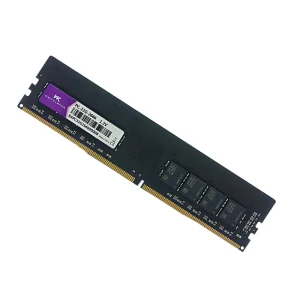
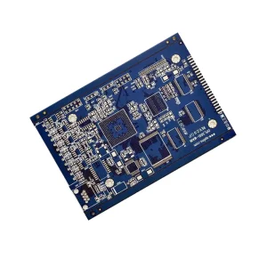
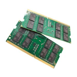
Get in touch with our engineering team for stencil aperture optimization, Gerber review, and customized PCBA production layout configurations.
 Kryntel