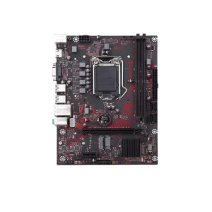
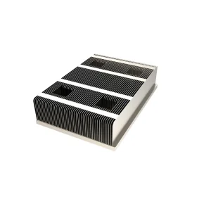
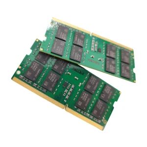
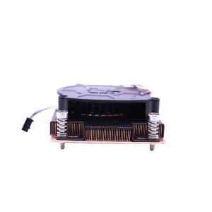
Explore our core high-performance semiconductor components and server thermal management modules manufactured under strict quality standards.
Engineering White Paper on High-Yield Solder Paste Printing & Precision Tooling
In the rapidly evolving landscape of surface mount technology (SMT), the yield rate of high-density Printed Circuit Board Assemblies (PCBAs) is determined in the initial stages of assembly. Industry data shows that up to 60-70% of all SMT defects are directly traced back to the solder paste printing process. As component footprints scale down to 01005, micro-BGAs, and ultra-fine pitch QFN packages, standard stencil-making techniques no longer suffice. High-precision laser-cut stencils have emerged as the industry standard, providing the dimensional stability, aperture wall smoothness, and aspect ratio tolerances required to support zero-defect printing operations.
As a global leader in high-performance hardware components, Kryntel Memory Technology (China) Co., Ltd. leverages its 9 years of overall semiconductor-related manufacturing and deep design engineering expertise to deliver robust, high-volume production stencils. With a dedicated engineering team, Kryntel integrates advanced CAD CAM file validation, fiber laser machining, electropolishing, and nano-coatings to supply stencils tailored for complex PCBAs—including DDR5 RAM modules, multi-layer server motherboards, and high-frequency communication boards.
Technical comparison of stencil technologies and performance indicators
Selecting the appropriate stencil fabrication technology is critical to resolving common manufacturing challenges such as bridge defects, insufficient paste volume, and solder balls. Below is the technical breakdown highlighting why high-precision laser-cut stencils with optional electropolishing and nano-coating outclass traditional chemical etching methods:
| Performance Indicator | Chemically Etched Stencils | Standard Laser-Cut Stencils | Kryntel Electropolished Laser Stencils | Advanced Nano-Coated Laser Stencils |
|---|---|---|---|---|
| Aperture Wall Profile | Concave (Hourglass shape) | Tapered (Trapezoidal) | Tapered & Smooth (Ra < 0.8μm) | Tapered with Hydrophobic Barrier |
| Minimum Pitch Size | > 0.5 mm | 0.3 mm | 0.25 mm | 0.20 mm (01005 components) |
| Release Efficiency | 60% - 70% | 75% - 80% | 85% - 90% | > 95% (Ideal for high yield) |
| Aperture Tolerance | ±15 μm | ±5 μm | ±3 μm | ±2 μm |
| Underside Cleaning Cycle | Every 1-3 prints | Every 5 prints | Every 10-15 prints | Every 30-50 prints (Boosts UPH) |
By utilizing specialized Fine Grain (FG) steel foils and state-of-the-art laser machinery, Kryntel ensures that each aperture features an engineered trapezoidal opening (typically 1% to 2% larger on the squeegee-contact side than on the PCB contact side). This physical shape optimization dramatically improves paste transfer efficiency, particularly when printing fine-pitch BGAs (Ball Grid Arrays) and small form-factor passives.
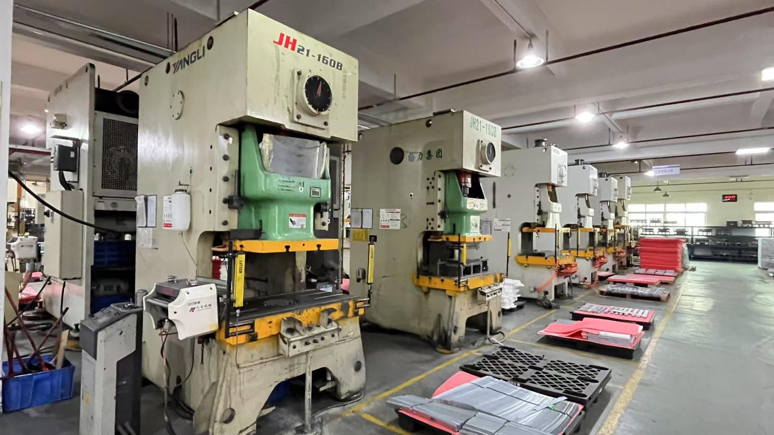
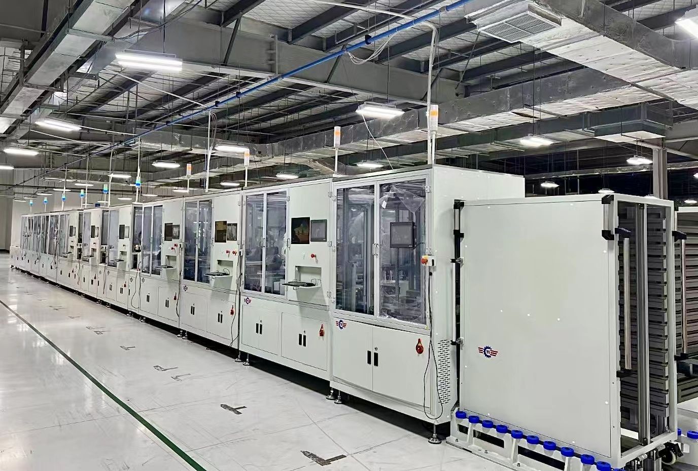
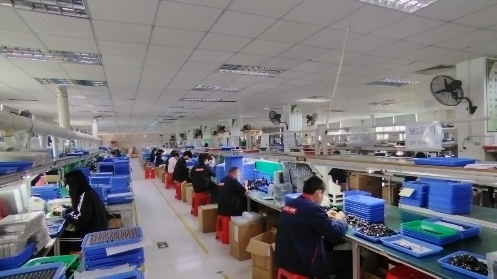
Our facility relies on strict multi-stage inspection standards and high-yield semiconductor assembly techniques
At Kryntel, our SMT stencil and PCB tooling solutions are built upon a rigorous 4-step quality assurance program. The QA division, staffed by 42 dedicated quality specialists, implements incoming material verification on all stainless steel foils (specifically selecting medical-grade SUS304 and high-density SUS301 stainless steel). The laser cutting path is optimized programmatically to calculate thermal expansion vectors, eliminating heat deformation during high-speed laser operations.
Incoming inspection of SUS304/SUS301 steel foils. Uniform thickness validation to prevent volume variations across the board layout.
Fiber laser system running under continuous climate control, limiting thermal drift to under 0.05% during large-panel cutting.
100% optical inspection verifying every aperture dimension and wall roughness, comparing CAD coordinates to the physical cuts.
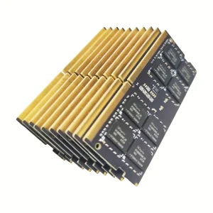
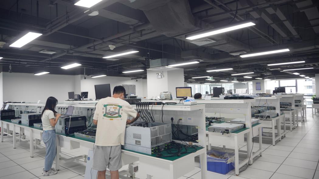
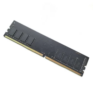
Our engineering department is comprised of over 160 specialists covering signal integrity, hardware architecture, mechanical modeling, and high-frequency PCB board reliability. This engineering scale enables Kryntel to assist customers during the DFM (Design for Manufacturing) review process. By analyzing the copper distribution, pad geometries, and component layouts on complex assemblies (like our DDR4/DDR5 high-speed RAM modules and Multi-Socket Server Motherboards), we optimize the aperture designs of SMT stencils before fabrication begins, reducing defect risks from the very first run.
Unlocking unparalleled manufacturing efficiency, cost structures, and global supply chain integrations
Partnering with an experienced Chinese SMT toolmaker like Kryntel provides global hardware brands, system integrators, and electronics manufacturers with distinct operational advantages:
Our facility operates within close proximity to major raw material suppliers, frame manufacturers, and advanced surface-treatment chemical plants. This localized synergy ensures reliable lead times, even during peak global electronics manufacturing seasons.
Time-to-market is everything. Our modern facility and high-capacity fiber laser tools allow us to process GERBER or ODB++ files, perform precision laser cutting, execute post-treatment, frame, pack, and export within 24 to 48 hours of file confirmation.
By combining advanced robotic handling systems with competitive engineering operations, we provide SMT stencils, heatsinks, and custom substrates with significant unit cost reductions compared to local fabricators in North America or Western Europe.


Tailored aperture solutions for heavy industrial systems to ultra-miniaturized consumer devices
Precision laser-cut stencils are engineered specifically to match the unique copper weight, heat dissipation path, and component density of different applications. Kryntel's SMT design division addresses these needs through application-specific engineering:
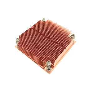
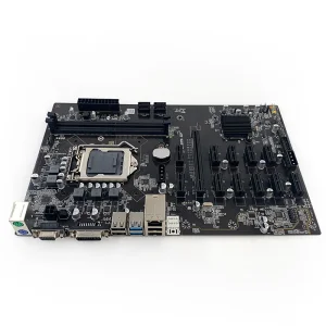
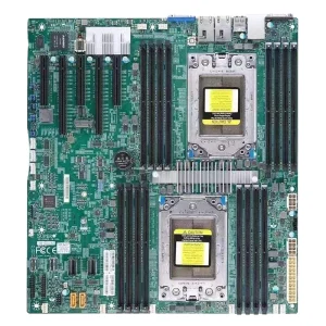
Server motherboards require variable solder volumes due to the presence of large multi-pin processor sockets alongside fine-pitch memory terminals. We design Step-Up / Step-Down stencils that provide localized thick areas for structural connectors and thinner zones for high-speed signal tracks, ensuring zero bridges and high structural reliability.
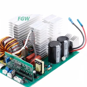
Heavy-duty industrial controllers, such as the ZX7-200/250 welding machine motherboard, require high solder volumes to withstand constant current stresses. We construct high-durability stencils from thicker steel foils (150μm to 250μm) with optimized thermal pad apertures to ensure complete joint coverage without solder voiding.
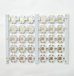
Aluminum PCBs for high-power LED systems (such as the T6 5050 and 3535 lamp bead series) present high thermal dissipation properties during operation. Solder paste printing on these surfaces must be extremely uniform. Our customized stencils for LED substrates implement gas-venting windowpane configurations, preventing gas entrapment under the components.
Serving tier-1 EMS providers, hardware brands, and distributors across 40+ countries
Kryntel Memory Technology (China) Co., Ltd. operates with a strong international logistics background. Our annual export revenues range from USD 8 million to USD 18 million, backed by a comprehensive supply network of 1,200 downstream and upstream partners. This extensive infrastructure enables us to coordinate international ocean, air, and express shipments efficiently. Whether shipping to SMT contract manufacturers in the USA, assembly facilities in Germany, or tech parks in India, Brazil, and the UAE, our products are packed in robust, ESD-safe wooden crates or structural foam packaging to ensure damage-free transit.
To streamline SMT line integration, our SMT stencils can be ordered with pre-mounted framing structures compatible with major printer platforms (DEK, MPM, GKG, and Ekra). We also offer space-saving frameless stencils designed for quick-release systems like Vectorguard.
Technical answers resolving common solder paste release, design calculation, and fabrication questions
We strictly follow the IPC-7525B stencil design guidelines. To achieve reliable solder paste release, the Aspect Ratio (width of aperture / thickness of stencil foil) must be greater than 1.5, and the Area Ratio (area of aperture / area of aperture walls) must be greater than 0.66. If the design exceeds these metrics, our design team works with the client to suggest localized micro-reductions or recommend hydrophobic Nano-coating options.
Fine Grain steel has a highly refined microcrystalline structure (crystal size of 1-2μm compared to 10-15μm in standard SUS304). During laser cutting, this structure reduces micro-burrs and produces extremely smooth aperture edges. FG steel minimizes friction between the solder paste and the aperture walls, resulting in a cleaner print release, especially for ultra-fine-pitch components down to 0.3mm.
Yes. We utilize precision micro-chemical etching and laser-cladding techniques to fabricate step stencils on single metal sheets. This allows us to combine thinner sections (e.g., 100μm for fine-pitch QFNs) with thicker sections (e.g., 180μm for large connectors) on the same board layout, ensuring the correct solder deposit volume for every component.
Our advanced Nano-coating is a hydrophobic and oleophobic layer applied via chemical vapor deposition. This coating repels flux chemistry, preventing solder paste buildup on the underside of the stencil. This reduces cleaning requirements (from once every 3-5 cycles to once every 30-50 cycles), saving solvent costs, extending stencil service life, and boosting line throughput.
We accept all industry-standard CAD formats, including Gerber RS-274X, Extended Gerber (GBR), ODB++, and DXF/DWG files. Our engineering team reviews the provided layouts to verify fiducial markers, squeegee path clearance, and paste release margins before starting production.
Each stencil is placed in a protective static-shielding sleeve, secured with rigid foam inserts, and packed in reinforced, custom-sized plywood crates or high-impact cartons. This double-layer packing system protects the tension of the stencil mesh and prevents physical warping or damage during sea or air transport.
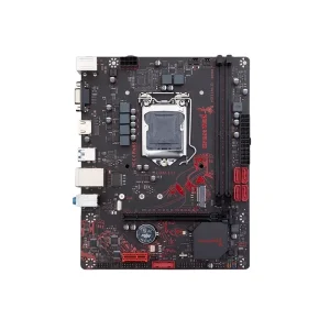
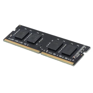
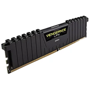
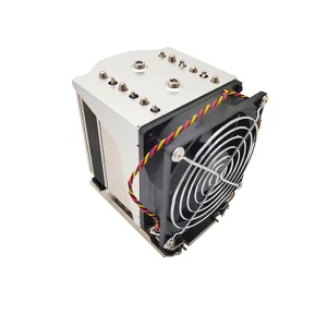
High-speed system memory modules, original computer motherboards, and server cooling systems
 Kryntel