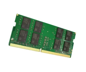
Engineered to support heavy current loads, fast switching speed, and intensive processing platforms across Victorian projects.
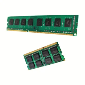
As Victoria continues to spearhead Australia’s transition toward advanced manufacturing, clean energy grid modernization, and localized defense system fabrication, the need for robust electronic hardware has surged. In Melbourne's thriving industrial corridors—from Dandenong's heavy transport hubs to the high-tech defense complexes near Geelong and Fishermans Bend—electronic reliability under harsh mechanical and thermal stresses is paramount.
Standard printed circuit boards with conventional 1oz (35µm) copper weights are no longer sufficient to handle the modern electrical loads required by today's localized projects. Heavy/Thick Copper PCBs—featuring copper weights ranging from 3oz to 20oz—are now the benchmark engineering solution. They prevent excessive thermal accumulation and minimize voltage drops across critical control interfaces, ensuring high reliability under Australia's stringent operating conditions.
With massive infrastructure commitments like the Melbourne Metro Tunnel Project, EV fleet transformations by the Victorian Government, and utility-scale solar arrays in regional Victoria, procurement departments require highly compliant, durable PCB layouts. Kryntel Memory Technology (China) Co., Ltd. coordinates direct, secure hardware links to supply heavy copper boards that resist degradation, survive prolonged thermal fatigue, and ensure operational longevity.
Maximizing system uptime by managing electrical current density and heat dissipation across thick FR4 profiles.
By increasing the copper thickness from 1oz to 4oz or more, designers significantly lower trace resistance. This directly drops localized I²R power loss, preventing structural delamination of the dielectric layer when subjected to high ambient heat waves in regional Victorian installations.
Heavy copper thickness in through-holes improves mechanical strength in high-vibration applications such as industrial mixers, train bogeys, and utility line switchgear. Thick copper plating inside the vias prevents thermal expansion fractures (CTE mismatches) across multilayer structures.
| Nominal Copper Weight (oz/ft²) | Target Foil Thickness (µm) | Estimated Max Current (A) for 10°C Temp Rise (Trace Width: 10mm) | Key Applications in Melbourne Industries |
|---|---|---|---|
| 3 oz | 105 µm | ~ 28 A | Heavy-duty LED drivers, industrial controls, high-speed telecom switches. |
| 4 oz | 140 µm | ~ 36 A | Automotive electronics, solar power inverters, secondary power distribution. |
| 6 oz | 210 µm | ~ 50 A | Railway power units, heavy welding machinery controls, defense arrays. |
| 10 oz - 20 oz | 350 - 700 µm | > 90 A (Engineered) | High-power grid relays, large EV battery charging stations, motor controllers. |
Our heavy copper PCBs are explicitly tailored to address the unique commercial and environmental demands of Melbourne's engineering sector:
For Melbourne systems integrators, relying solely on local prototyping workshops often results in production delays and high scaling costs. Kryntel Memory Technology (China) Co., Ltd. provides the ideal balance: high-precision Chinese fabrication combined with robust export pathways directly to the Port of Melbourne.
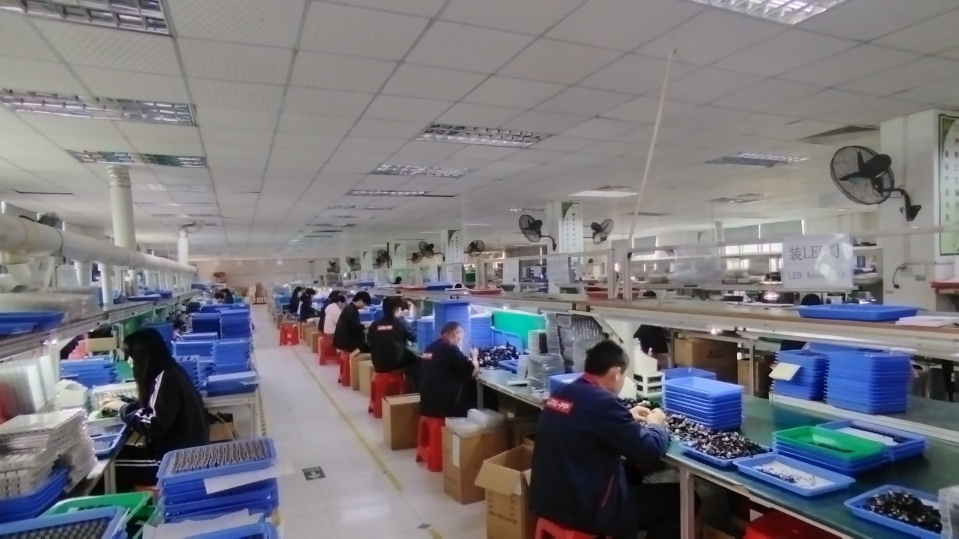
Founded in 2016, Kryntel has established itself as an industry leader in complex hardware assemblies and high-reliability circuitry. Spanning an expansive production footprint and leveraging a vast network of 1,200 upstream and downstream component partners, we secure high-grade raw materials (like high-Tg FR-4, copper foils, and thermal interface materials) even during global market shifts. This direct pipeline guarantees stable prices, material consistency, and rapid production cycles for our Victorian clients.
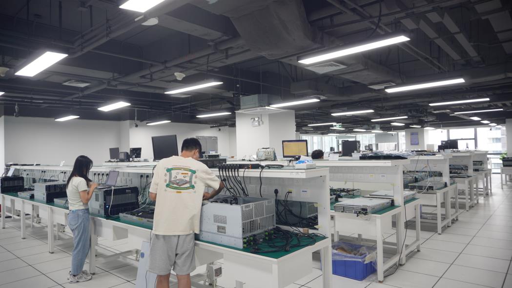
Our quality assurance protocol includes multi-stage inspections overseen by a dedicated QA team of 42 professionals. Every high-current board undergoes strict evaluations: AOI (Automated Optical Inspection), thermal stress testing, high-pot isolation checks, and board-level micro-section analysis to verify plating thickness consistency in our state-of-the-art facilities.
Kryntel’s R&D department features 160 engineers specializing in PCB layout optimization, high-frequency design, signal integrity, and thermal dissipation systems. In the past year, we have successfully launched over 280 memory, motherboard, and substrate solutions, ensuring our clients stay at the cutting edge of electronic hardware technology.
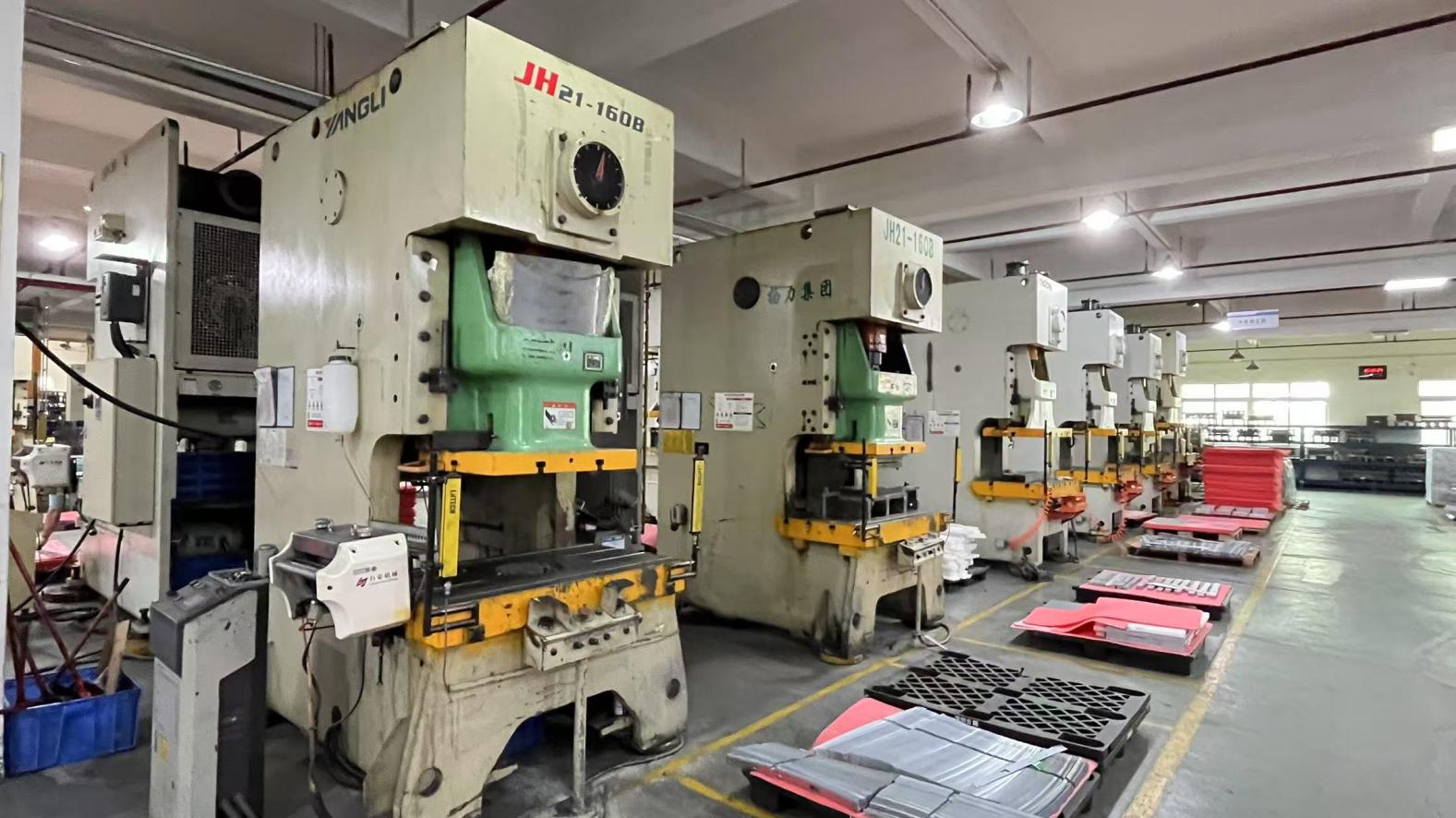
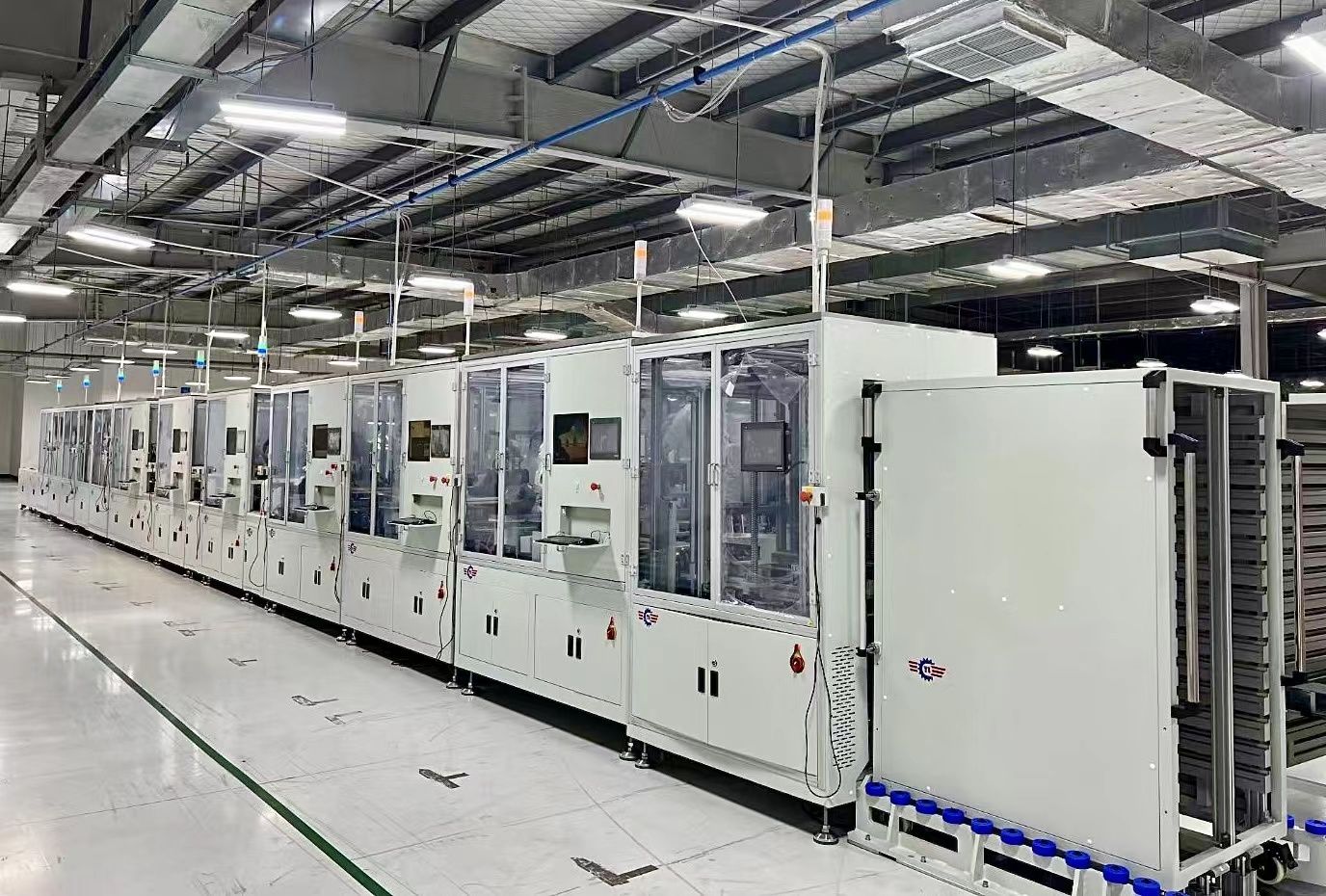


As power electronics shift toward higher efficiency in smaller enclosures, the integration of heavy copper paths into multi-layer configurations (embedded copper rails) is key. We are continuously refining our fabrication techniques to support this evolution:
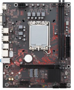
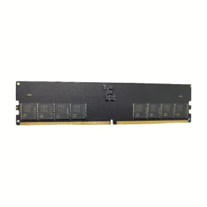
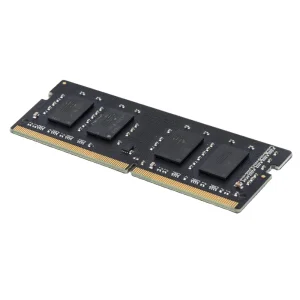
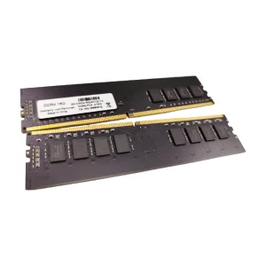
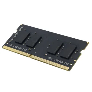
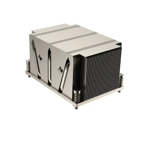
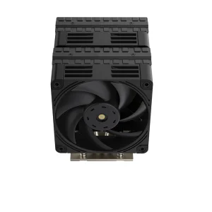
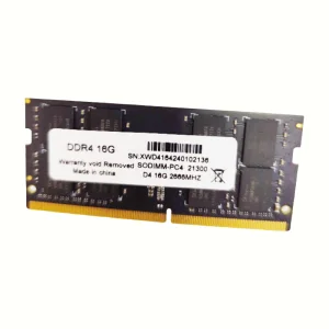
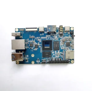
Explore our industrial-grade components, motherboards, heatsinks, and custom memory modules built for heavy industrial computing.
Working with an international factory should not mean experiencing logistics friction. Kryntel manages every step of the export pipeline. Supported by seasoned export compliance experts and offering sea freight options to the Port of Melbourne or express air courier deliveries to Tullamarine Airport, we ensure your components arrive safely and on time.
We work under clear DDP/CIF/FOB terms to streamline import processes. By providing complete technical data packets—including IPC inspection logs, impedance testing charts, certificate files, and solderability evaluations—we make sure Victorian customs clearance runs smoothly, keeping your manufacturing schedules right on track.
Frequently asked questions by electronics designers and procurement leads in Victoria, Australia.
Whether you are designing advanced solar grid infrastructure, heavy-duty industrial control motherboards, or specialty cooling assemblies, Kryntel has the engineering experience to deliver on time and to your specifications.
Send Inquiry Now Kryntel