Ensuring maximum solder transfer efficiency and zero-defect coplanarity across Brazil's premier electronics manufacturing lines.
Analyzing localized manufacturing mandates, technological demands, and stencil release physics.
Brazil's domestic electronics industry is heavily governed by the Basic Productive Process (Processo Produtivo Básico - PPB). This system mandates specific levels of local manufacturing and component insertion to secure tax reductions under the *Lei de Informática*. For global Tier-1 and domestic EMS (Electronic Manufacturing Services) providers in regions like the Zona Franca de Manaus (ZFM) and the technology hubs of Campinas and Sorocaba (São Paulo), local PCB assembly (PCBA) is not just an option—it is a regulatory and economic necessity.
However, importing finished, custom-cut laser stencils can introduce critical logistics bottlenecks. Any modification to a PCB design requires a corresponding stencil iteration immediately. Waiting for overseas air shipping stalls production lines. Kryntel Memory Technology addresses this challenge by combining robust Chinese high-volume engineering with direct express shipping, optimized CAD processing, and compliance protocols designed to clear Brazilian customs (Siscomex) rapidly.
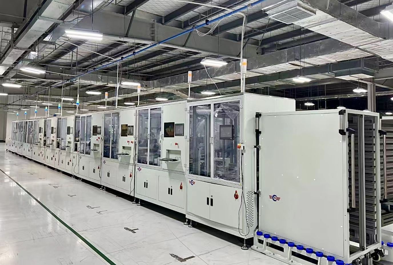
In modern high-density interconnect (HDI) boards, components such as 01005 passives, ultra-fine-pitch CSPs, and micro-BGAs require minuscule aperture sizes. SMT engineers recognize that over 60% of all solder defects (such as bridging, solder balls, and insufficient solder volume) originate directly during the paste-printing process.
Whether a stencil successfully deposits solder paste depends on the Area Ratio (AR), calculated as the area of the aperture opening divided by the area of the aperture walls. For reliable release, the industry standard dictates an AR > 0.66. When designs drop below this threshold, standard laser-cut stencils fail, necessitating specialized techniques like fine-grain stainless steel, chemical polishing, or nano-coatings. Kryntel’s engineering team reviews all incoming Gerber data against these physics guidelines before production begins.
From standard fiber laser cutting to localized nano-coatings and step stencils, we support the technical evolution of Brazilian PCB assembly lines.
Utilizing high-speed, thermal-stabilized fiber laser systems (such as LPKF setups), we cut fine-grain stainless steel sheets (SUS304/SUS355) down to thickness levels of 80µm–150µm, achieving ultra-smooth aperture walls and tapering designed to optimize paste release.
Designed for boards containing a mix of high-power components (requiring large paste volumes) and fine-pitch BGAs (requiring tiny paste volumes). Our chemical etching and precision micro-milling processes create step changes in stencil thickness (e.g., 150µm stepped down to 100µm) with gradual, uniform ramp profiles.
Applying a proprietary nanoscale polymer coating to the contact side and aperture walls of the stencil. This coating repels solder paste, minimizes cleaning frequency (extending cycles from 1 wipe per 3 prints to 1 wipe per 15-20 prints), and significantly reduces bridging issues on 0.4mm pitch components.
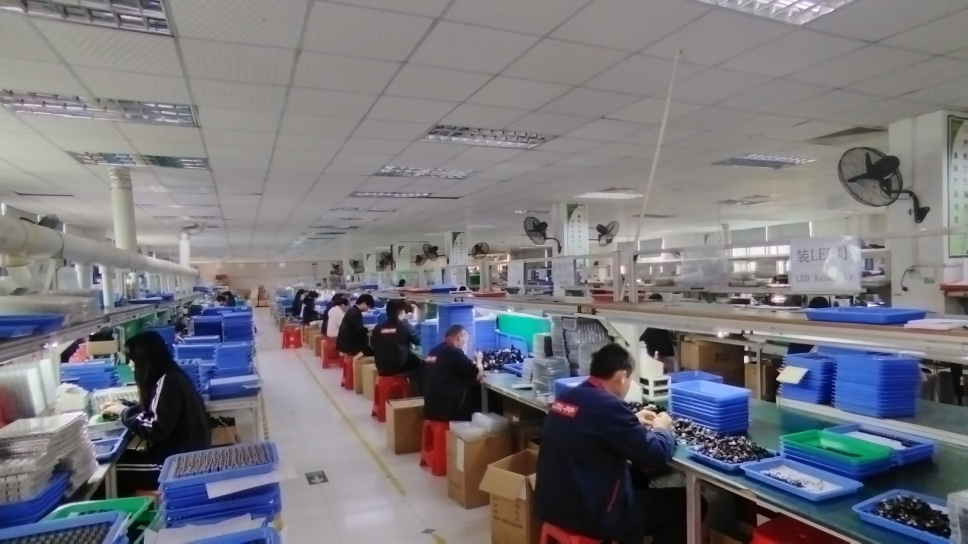
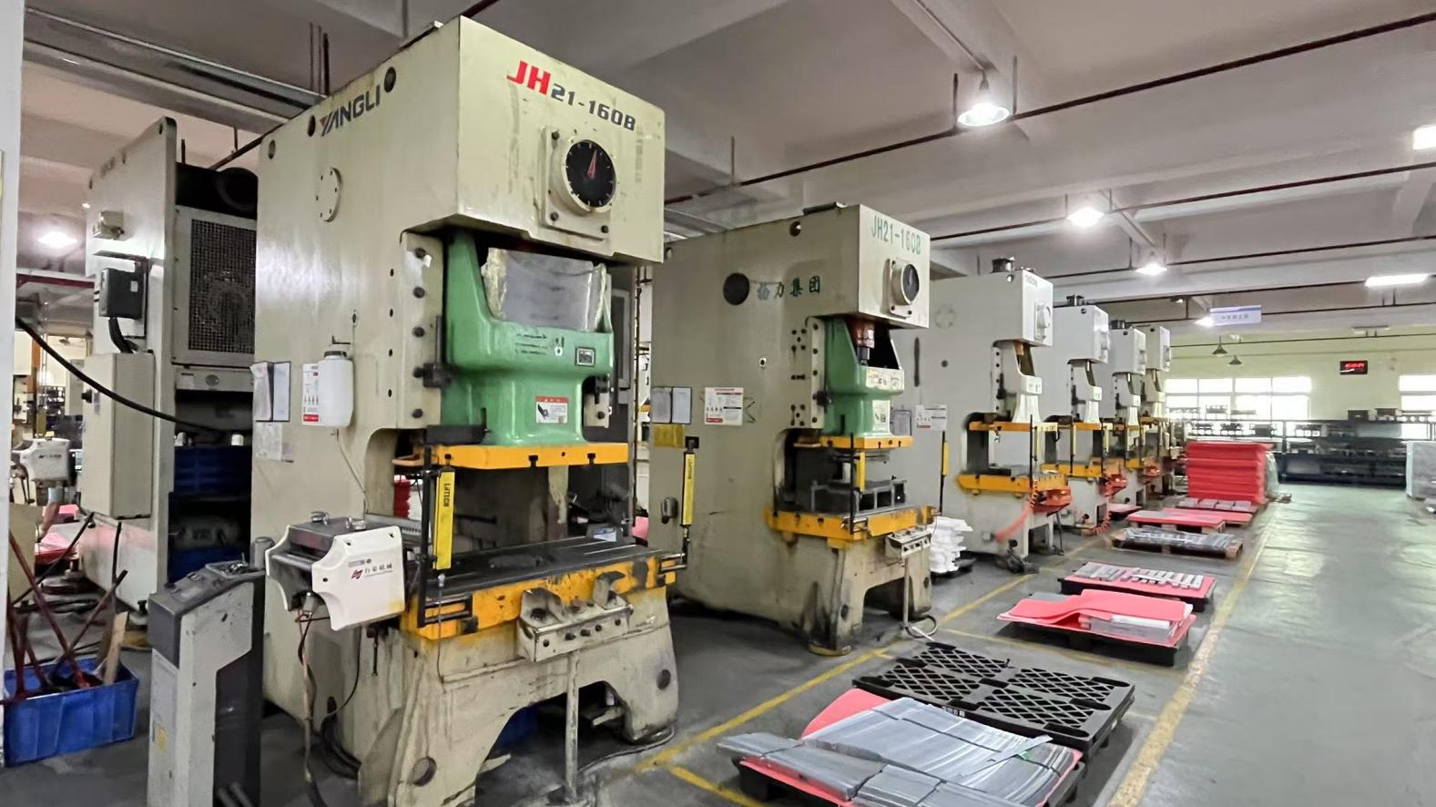
Operating a modernized facility in China, Kryntel Memory Technology (China) Co., Ltd. integrates production with Industry 4.0 automation. We source high-grade raw materials—including fine-grain tensioned steel sheets from Japan and Germany—to guarantee flat surfaces and consistent tension levels across frames.
Our quality management is built on rigorous multi-stage inspection procedures:
We tailor our aperture design geometries to meet the specific requirements of regional manufacturing clusters.
Automotive electronics demand compliance with strict thermal dissipation and safety standards. Our stencils feature optimized aperture geometries designed to reduce voiding under large thermal pads (such as QFNs and DPAK devices) down to under 10%. We use specialized cross-hatching and windowpane aperture designs to ensure reliable solder coverage without excess paste outflow.
High-volume assembly of smartphones, smart TVs, and smart meters requires extremely tight stencil tolerances. For BGA pitches down to 0.35mm, our electroformed or nano-coated laser stencils prevent bridging and pad starvation, maintaining high yields and reducing rework costs on high-speed SMT placement lines.

Navigating Mercosur tariffs and Siscomex logistics to ensure uninterrupted production schedules.

Importing industrial tooling into Brazil can present administrative challenges. Kryntel’s export teams are highly experienced in managing logistics for the Brazilian market. We provide comprehensive, accurate documentation—including HS Codes (NCM) and proforma invoices matching Siscomex requirements—to facilitate customs clearance under local RADAR licenses.
To protect delicate fine-mesh stencils during transit across changing climates, we package all shipments in vacuum-sealed, moisture-barrier bags with desiccant packs, secured inside rigid, shock-absorbing wooden crates. This ensures your stencils arrive flat, clean, and oxidized-free, ready to mount on your DEK, MPM, or Ekra printers.
Connect with our SMT application engineers today. Submit your Gerber files (ODB++ or RS-274X) for a free design-for-manufacturability (DFM) review and pricing quote.
Send Inquiry NowDiscover our range of memory solutions and turnkey PCBA prototypes optimized for Brazil's manufacturing sectors.
Combining high-speed production facilities with rigorous quality management systems.
Established in 2016, Kryntel Memory Technology (China) Co., Ltd. is a specialized OEM/ODM manufacturer focused on high-performance SMT assembly and precision memory components. Backed by a team of 160 engineers specializing in signal integrity and board layout, we support the manufacturing needs of global brands, system integrators, and electronics distributors.
Our quality control system spans incoming material inspection, in-process checking, high-temperature aging tests, and final automated testing. With a dedicated QA team of 42 professionals, we ensure each production batch meets precise technical standards, minimizing line failures for international partners in the United States, Germany, India, Brazil, and the UAE.
Answers to technical, logistical, and compliance questions for importing SMT stencils and PCBAs to Brazil.
Standard laser stencil cutting requires 24 to 48 hours following CAD data verification. Express air shipping to locations in São Paulo, Campinas, or Manaus typically takes 5 to 7 business days, depending on customs processing speeds.
We calculate the Area Ratio (AR) for each aperture design. When a board mixes large power devices with fine-pitch BGAs, we recommend step-down stencils. This allows us to reduce the stencil thickness locally (e.g., from 150µm to 120µm) in fine-pitch zones while maintaining sufficient paste volume elsewhere.
Nano-coatings create a solder-phobic barrier on the stencil’s underside and inside the aperture walls. This improves paste transfer efficiency, reduces under-stencil wiping frequency, and minimizes the risk of bridging and solder balls on small pads.
We provide complete documentation, including NCM classifications, commercial invoices, and packing lists matching Siscomex standards. This helps prevent delays and ensures smooth customs clearance under your company's RADAR license.
 Kryntel