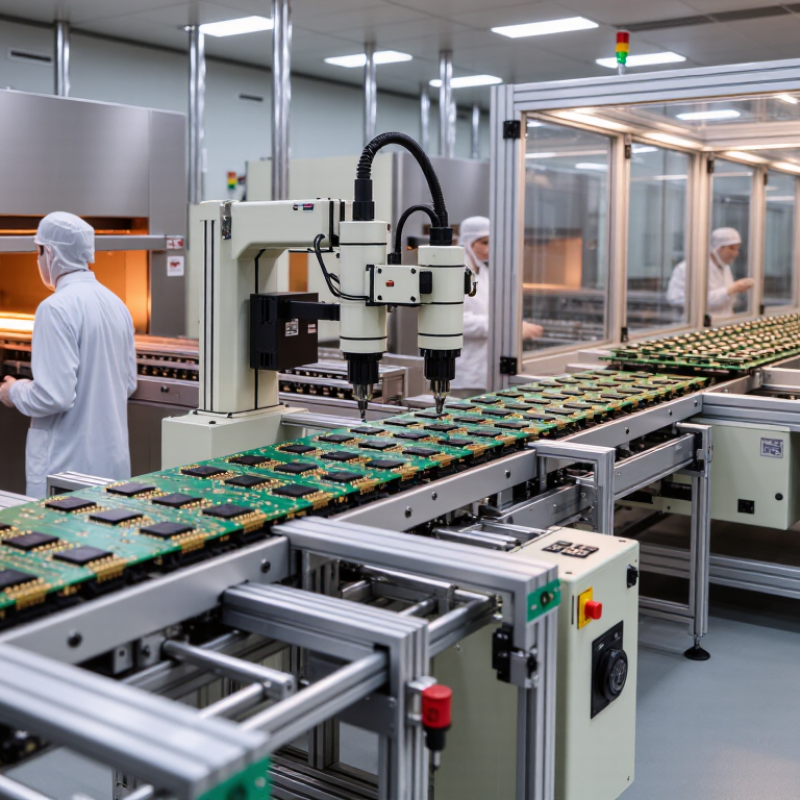
A memory module may look simple: a green board, several black packages, and a row of gold contacts. Its manufacture is a tightly controlled sequence. In 2026, the Memory module manufacturing process typically combines component sourcing, printed-circuit-board production, surface-mount assembly, firmware programming, and electrical testing. Small tolerances matter. A misplaced component or weak solder joint can cause failures that appear only under heat or sustained workloads.
The market scale makes manufacturing quality consequential. Gartner reported that worldwide semiconductor revenue reached $626 billion in 2024, up 18.1% from 2023. That figure covers semiconductors broadly, not memory modules alone, so it is useful context rather than a module-market estimate. JEDEC’s DDR5 standard provides the technical framework for compatible memory devices and modules. Manufacturers then validate specific designs against system requirements, component specifications, and production test results.
SEMI CEO Ajit Manocha has publicly emphasized the importance of resilient semiconductor supply chains and continued investment in manufacturing capacity. In paraphrase, his point is that reliable production depends on more than equipment: it also requires skilled teams and dependable suppliers. The factory details are less glamorous. Pick-and-place machines position tiny components; reflow ovens melt solder; automated optical inspection checks alignment and joints. Final tests verify operation across voltage, timing, and temperature conditions. A passing test is not the whole story. Traceability, process monitoring, and corrective action help teams understand defects and improve yield. The process is sophisticated, but not infallible. That gap deserves attention.
DRAM wafer fabrication begins with a 300 mm silicon wafer, a polished disk about the width of a large dinner plate. Its surface must be exceptionally flat and clean. Even a speck of dust can interfere with a tiny circuit feature. Small particles matter. In a cleanroom, engineers build patterns through repeated steps such as photolithography, material deposition, etching, and controlled doping. Each cycle adds or shapes part of the device structure. The sequence is precise, but not effortless; process conditions need frequent measurement and adjustment.
Within each memory cell, a transistor controls access to a capacitor that stores electrical charge. Creating these structures across a wafer requires careful alignment between many patterned layers. Inspection tools check dimensions and look for defects, while electrical tests help identify working areas before the wafer is cut into individual dies. Results can vary across a single wafer, so manufacturing teams track both yield and consistency. The scale is impressive, though the process can seem almost stubbornly sensitive: a slight shift in a layer may affect thousands of cells. That is one reason wafer fabrication deserves more attention than the finished module alone.
At wafer probe, a tester touches each exposed die through tiny metal needles. It checks whether circuits work, how much memory each die holds, and how quickly it operates. Results appear as a wafer map, with each die assigned a grade or marked for rejection. A weak contact can imitate a bad circuit, so operators watch probe marks and retest suspicious readings.
These grades answer different questions. Functionality checks for failed cells and circuit faults. Density confirms usable storage capacity after repairs and redundancy are considered. Speed grading measures timing under specified voltage and temperature conditions. Dies that pass may still fall into different performance bins. Probe data guides sorting; it does not guarantee final packaged-device performance.
The World Semiconductor Trade Statistics organization reported global semiconductor sales of $627.6 billion in 2024, with memory sales rising 78 percent. That demand makes accurate die recovery valuable, but aggressive grading can misclassify marginal parts. The map is useful, not infallible. Tips: Keep probe-card contact stable, log retests, and compare wafer-sort results with package-test data. A little drift matters.
A 288-pin DDR5 UDIMM starts as a carefully routed printed circuit board. Its edge contacts connect the module to the motherboard, while copper traces carry signals between components. The board is made with controlled spacing and multiple conductive layers. Small differences in trace length can affect signal timing. The details matter.
Packaged DRAM chips, rather than bare silicon dies, are placed onto the board using automated assembly equipment. A stencil applies measured solder paste to each pad. Pick-and-place machines position the DRAM packages and supporting parts, such as the SPD hub and power-management components. The populated board passes through a reflow oven, where heat melts the solder and forms electrical joints. Too little heat can leave a weak connection; too much can damage parts. Not every defect is visible. Automated optical checks look for misalignment, while additional inspection can examine hidden solder joints.
Each module is then tested for electrical behavior and configuration data. Testing can reveal faults that a clean surface cannot. A small placement error may cause intermittent problems, so inspection and handling remain important. Even well-controlled production has limits, and a test result should be interpreted alongside the module’s specifications.
How Are Memory Modules Manufactured in 2026?
After memory chips are mounted on a DDR5 circuit board, the module’s SPD memory is programmed with identification and operating data. This small data store tells the system which capacities, timings, and supported profiles are available. For a standard profile, the nominal supply is 1.1 V. The SPD does not supply that voltage; it reports settings that compatible system firmware can apply. Enhanced profiles may specify different operating conditions.
Programming needs more than copying a profile. Technicians check that timing values match the installed chips and board layout, then write the data and read it back. A valid checksum helps detect corrupted information, but it cannot prove that every setting works reliably. That part takes testing. Modules are checked across supported speeds and temperatures, since a clean bench result may not predict every system’s behavior. It is easy to trust a successful readback too much.
Tips: Confirm the voltage and timing fields against the module’s intended profile. Compare the programmed SPD contents with the approved production file, and test samples in compatible systems. Keep a record of revisions; small data changes can matter. One limitation remains: firmware behavior differs, so validation should not stop at the programming station.
In 2026, module validation should test both DDR5 subchannels independently, not treat a DIMM as one wide lane. JEDEC’s JESD79-5C DDR5 specification defines two 32-bit subchannels, giving a 64-bit data path on a standard non-ECC module. Test patterns should expose stuck bits, timing drift, and errors that appear only under sustained traffic. Small details matter.
ECC needs a separate check. On-die ECC corrects certain errors inside a memory chip; it does not replace system-level ECC across the module. Where module ECC is fitted, validation should confirm check-bit handling and report corrected and uncorrected errors under load. JEDEC’s DDR5 specification and module design documents provide the technical basis for these checks. A pass at room temperature is not enough.
Thermal testing should follow the exact component and module operating limits, since no single temperature ceiling applies to every design. Log sensor readings during repeated writes, then retest at the specified temperature range and data rate. JEDEC temperature-grade requirements help define that range. A small airflow change can shift readings. One weak spot remains: short bench tests may miss errors that emerge after hours of heat soak, so validation records should include test duration, ambient conditions, and failure counts.
Tiny metal needles contact each exposed die. The tester checks circuit function, usable memory capacity, and operating speed. Contact marks matter.
Results appear on a wafer map. Dies receive grades or rejection marks based on test results. The map can still be wrong.
A weak probe contact can look like a circuit fault. Operators review suspicious readings and record retests. Small drift matters.
No. Wafer results guide sorting, but packaged-device performance can differ. Final package testing adds useful evidence.
Automated machines place packaged chips and supporting parts onto solder paste. A reflow oven melts the paste and forms electrical joints. Heat must be controlled.
Optical checks can detect misplaced parts. Other inspections examine hidden solder joints. A clean surface proves little.
A standard non-ECC module has two 32-bit subchannels. Separate tests can reveal stuck bits, timing drift, or errors during sustained traffic.
On-die correction and module-level ECC are different functions. Where module ECC is fitted, tests should track corrected and uncorrected errors under load.
Short room-temperature tests may miss faults after hours of heat soak. Record sensor readings, airflow, test duration, and failure counts. Still, no test catches everything.
The Memory module manufacturing process begins with DRAM circuits formed on 300 mm silicon wafers. After fabrication, each wafer is probed to identify working dies and sort them by capacity, functionality, and speed grade. This testing helps determine which chips are suitable for particular module configurations before they are separated and prepared for assembly.
Selected DRAM chips are mounted on a 288-pin DDR5 UDIMM circuit board, then the module’s SPD data is programmed with its operating profiles for a nominal 1.1 V supply. Final validation checks that the module’s two 32-bit subchannels operate as intended, verifies optional error-correction features where included, and evaluates performance against thermal limits. Together, these stages turn tested silicon into a configured memory module ready for system-level use.

Kryntel